This thread has been locked.

If you have a related question, please click the "Ask a related question" button in the top right corner. The newly created question will be automatically linked to this question.

BQ24296M Failure: Short between SW and GND due to LSFET Overvoltage Damage

Other Parts Discussed in Thread: BQ24296M

Hello,

We are using the BQ24296M as a battery charger/controller, and have had several units that fail with a short between the SW and GND pins.  We had a third party lab take some SEM pictures after decapsulating the failed ICs, and we are pretty sure the damage is at LSFET (Q3 in the datasheet).  Based on the pictures, which show no other damage, deformation, etc., on Q1, Q2, Q4, etc., and also because LSFET has a pretty low absolute maximum rating, we think the cause is an over-voltage event.

We are still coming up with a list of operating conditions that cause the issue, but we have at least one unit that failed without plugging/unplugging the charger.

The part is used with a 3.7V, 8200mAh Li-Ion Battery.  On-the-go operation is hardwired off (i.e., OTG pin tied to ground).  The nominal charger voltage is 5V and our board has reverse-voltage protection (up to -24V) and over-voltage protection that starts cutting off the input voltage to the BQ24296M if Vin exceeds 9V.  

Also, Ilimit is set to 2.4A max with a 180 Ohm resistor from ILIM to ground.

So, my question is whether you guys have seen over-voltage failures at LSFET in the past, and if so, under what conditions?

I will update this post as we make additional measurements this coming week.

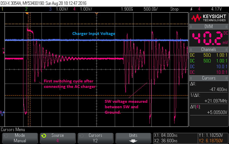
Update #1: The attached screenshot is the behavior when you first plug in an AC charger (to Vbus) (Even though the Input voltage looks like a solid DC voltage, it has just risen from 0V to 5V a short time berfore, which is not shown on the screen). That very first switching cycle sure looks like the FETs are switched in boost mode, with the voltage at the SW pin rising above both Vbus and VBAT.  I'm not sure this is related to our issue, but thought it's interesting since the OTG pin is hard tied to ground.

  • Referring to page 5 of the d/s, 

    1)SW/BAT/SYS pins have lower voltage ratings than VBUS/PMID pins.
    2)When converter is switching, SW pin sees the same voltage as VBUS/PMID voltage.
    3)High and fast input voltage spikes may damage the device and cause SW pin short to ground.
    It is recommended to add a good TVS diode with fast response time and accurate breakdown voltage for VBUS.
    Thanks,
    Ning.
  • Hi Ning,

    To address your comments:

    * As I mentioned in my original post, we do have over-voltage protection on Vbus, including both a TVS and some active circuitry to cut off any input voltage above 9V (which is well below the maximum allowed input on Vbus)

    * I assume that as long as Vbus is kept under its maximum input voltage rating, the SW pin should not be damaged.

    * Also, please see my screenshot in the original posting - you can see that under some conditions, the voltage on SW is indeed greater than the voltage on Vbus.  

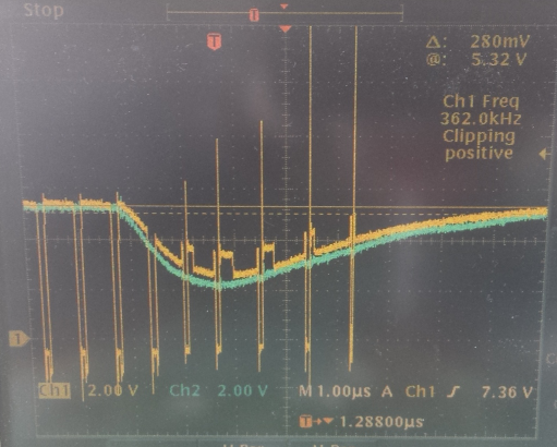
    * Furthermore, We have seen that if the voltage on Vbus drops, even well below Vvbusmin (3.8V), the buck converter continues switching, generating some rather large voltage spikes on SW.  In the image below, the blue line is the Vbus voltage.  The dip is due to turning on another load.  As you can see, the voltage dips down to almost 2V and the converter does not stop.  In this case, the battery voltage is greater than the Vbus voltage so the converter is almost behaving like an uncontrolled boost converter for the few cycles it takes the Vbus voltage to recover.  Is this expected behavior?  If so, then it's not a matter of picking a good TVS for Vbus, but rather we'd be looking at a heavy snubber or even a clamp for SW.

  • Referring to page 5 of the d/s,

    1) VBUS has 15V max voltage rating when NOT SWITCHING. When the converter is switching, i.e. Q2 is turned on, SW pin voltage is the same voltage as VBUS/PMID voltage ideally. The SW spikes are due to parasitics in the system.

    2) SW pin has only 7V max voltage rating (8V for 20ns). So TVS etc to cut off any input voltage above 9V can't protect SW pin from damages when the converter is switching.

    I'm unable to comment on the large SW spikes you observed since I do not know your complete system and test setups.

    Thanks,

    Ning.

  • Hi Ning,

    Yes, I do understand the absolute maximum limits and the fact that the voltage at SW is equal to VBUS when the part is switching.

    I would expect the converter to immediately STOP switching when the Vbus voltage rises above Vacov or falls below Vvbusmin.  We verified that it does stop when going above 6.6V (Vacov), but as you can see my the image in my previous post, the voltage dips almost to 2V, which is well below Vvbusmin (3.8V typical), and the converter is still switching.  Is this expected behavior?

  • There is response time for VBUS OVP. If the VBUS transient is faster than VBUS OVP, the SW pin could be damaged before the VBUS OVP takes action.

    The device is guaranteed to operate above 3.9V, but it may work below 3.8V. Refertting to pagge 7 of the d/s, the typical VVBUSMIN is 3.8V.

    Thanks.

  • Hi Ning,

    We would like to share some additional data we have to verify that we have truly identified the root cause of the issue. Some of this data is going to be very interesting to the original design team for this part. It shows what we believe is a valid use case for the part, that under some use cases could result in reliability problems.

    We would prefer to not share this on a public forum. Can you please organize a 15-20 minute conference including yourself and other team members at TI who may be interested in this?

    Once we are certain we have identified and fixed our issue, I would be happy to post our conclusions here for the benefit of anyone else who may be having similar issues.

    Thanks!
  • Could you please email additional info and data to me at n-tang2@ti.com and let me take a look first?

    Thanks!