This thread has been locked.

If you have a related question, please click the "Ask a related question" button in the top right corner. The newly created question will be automatically linked to this question.

BQ33100 4 cell questions

Other Parts Discussed in Thread: BQ33100

Hello,

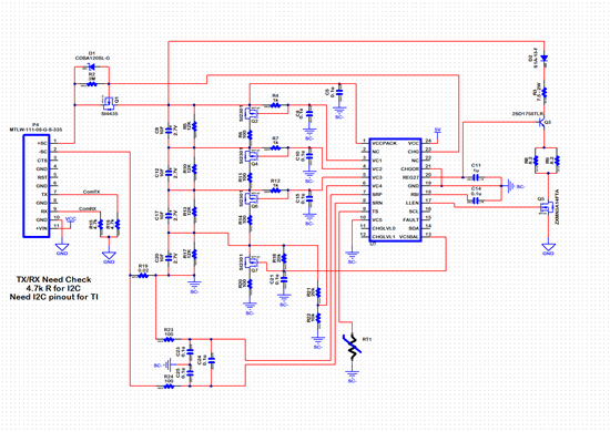
We are working on a supercap backup circuit that uses the TI BQ33100.  While the EVM shows examples for a 5 cell setup, we  have a 4 cell setup, and have a few questions that we can't answer using the datasheet and EVM user guide.  We based most of our design off the diagram on page 11 of the datasheet, and I'll refer to those component reference designators. Also, here is my design so far.

  1. In the eval datasheet, there is a voltage divider using (R32) and (R33) which connects to VC5. In my design since I only have 4 caps and per the datasheet on a 4P setup, I grounded VC5 and rerouted this voltage divider output to the VC4 pin which on my sheet is R21 and R22.  Did I make the right assumption? 
  2. We only have 1 pin for power in/out of the board.  Power will be provided for charging when the main supply is working, and then we provide power out when that power goes away.  On the EVM, the input and output are separated on (TB1) and  (J1). TB1 is separated from the circuit using (Q6) to control the charge process. In my diagram (Q6) is Q1 and in order to allow both input and output of power on the SC+ power pin, I added the shotkey diode D1 to allow controlled charging by the BQ33100, but then allow power to freely flow back to the device during a power failure. Is using that bypass diode an acceptable way to set up a single connection for both charging and discharge? Would this cause any problems that you are aware of?  Do I need back to back FET's?
  3. Next, the 5V power supply is going to be supplied from a separate 5V source that comes in from the +VIN pin on the interface connector P4 and then gets regulated to a steady 5V using an LDO on this board. On the eval board, the power supply for the BQ33100 gets its power from the system input (TB1) which is active when the charge power is on. On my board, the BQ33100 may have power from the 5V circuit even though there is no net positive energy on the SC+ line to actually charge the caps, and instead it would be in discharge mode. Would this cause any strange behavior with the BQ33100 such as it thinking there is a charging fault or something similar? 
  4. Finally, I am not exactly sure what to do with the CHGLVL0/1 and am not sure if I even need them since I am not using the on-board charging circuit. Do I need to do anything special with those?

Thank you,

JC

  • Hi Jamal,

    1. I see you have external balancing resistors in parallel with your caps. In that case, there will be no need for the  balancing fets and you will need to operate the device in stack mode of operation. Pls see the data sheet for operating the device in stack mode of operation. In stack mode, the individual nodes of the caps will not be connected to the voltage input pins of the ics. Only the top and the bottom of the stack will. However, if you will not be using the stack mode and would rather use the balancing functionality of the device since you have four caps, you will need to eliminate your 12 k resistors which you have in parallel with your caps. Also VC5bal will have to be grounded as well as VC5 and not as you currently have it. See page 11 of the data sheet.

    2.I would not have the discharge path to your application from the caps go through the charge fet because there might be instances where the device might turn the charge fet off, yet your application needs power from the caps. I suggest sticking to the EVM schematic or come up with a solution whereby the discharge path doesn't go through the fet.

    3. I don't believe powering the chip that way would cause an adverse effect. but i think its the circuit is an overkill. when not being powered by the charger, the device on our evm can also get power from the caps. the advantage of yours is that even if the caps are fully discharged, and there is no charge current, the device will still have power and be able to relay accross measured values.

    4.please review the charging section of the data sheet and user guide for the device. those voltage levels are necessary to be able to increase the lifetime performance of your caps. with the help of those and the feedback resistors to your charging circuit, you can regulate the voltages your caps will be charged to. It is a known fact that charging caps to a lesser voltage .i.e 2.1 V per cap will increase the lifetime of the caps. When they age and ESR increases and capacitance reduces, you charge them to a higher voltage (max 2.7 V depending on the cap) to be able to squeeze more juice from them.

    thanks

    Onyx

  • Hi Onyx,

    Thanks for your help.  We have a few more questions for you...

    1.  When we have the voltage jump from the normal charging voltage to a learn voltage, what minimum change is needed for the system to jump to and then drain down to the normal charging voltage in order to get a proper learning cycle? (Diagram of this on datasheet p14)

    2. We program in the voltages into VCHGA,VCHGB, ect that each stage of the charging circuit outputs depending on the CHGLVL pins. What level of accuracy is required between what we tell the BQ33100 the voltage will be vs. what our power supply will actually put out?  We are hoping not to have any major calibration requirements, and instead be consistently within a target range for each board produced. 

    3. In relation to my first question, what voltage option will the BQ33100 generally choose when it is running a learn cycle? Will it just jump to the maximum voltage allowed, or does it only choose the necessary difference to get a good reading?  Am I also correct to assume that when we set VLEARNMax, that instead of setting the power supply directly, it is just choosing one of our 4 charging options that fall below the limit during the learn process?

    4. Do we need to preform a calibration on each board produced for the IC to be able to complete its expected job? If we need to calibrate each and every board, it could cause delay problems. What type of margin of error would be expect from most of these devices in an uncalibrated state?

    5. Finally, do you know how long the learning process usually takes on these units?

    Thank you very much!

  • 1.  When we have the voltage jump from the normal charging voltage to a learn voltage, what minimum change is needed for the system to jump to and then drain down to the normal charging voltage in order to get a proper learning cycle? (Diagram of this on datasheet p14)

    Ans: The learning occurs during discharge after charging to vlearnmax and the voltage delta required for learning is programmable in the data flash. The parameter is the learn delta voltage. the default is 500mV which is usually ideal for most applications. The idea is such that there are enough voltage samples collected to ensure capacitance measurement accuracy

    2. We program in the voltages into VCHGA,VCHGB, ect that each stage of the charging circuit outputs depending on the CHGLVL pins. What level of accuracy is required between what we tell the BQ33100 the voltage will be vs. what our power supply will actually put out?  We are hoping not to have any major calibration requirements, and instead be consistently within a target range for each board produced. 

    Ans: The values you program in the data flash should correspond to the different voltage levels the charger outputs. You should use resistors with a tolerance of 1% or better in the feedback circuit of your charger which sets the charge levels.

    3. In relation to my first question, what voltage option will the BQ33100 generally choose when it is running a learn cycle? Will it just jump to the maximum voltage allowed, or does it only choose the necessary difference to get a good reading?  Am I also correct to assume that when we set VLEARNMax, that instead of setting the power supply directly, it is just choosing one of our 4 charging options that fall below the limit during the learn process?

    ans: During learning the voltage is set to the maximum voltage which is the Vlean max and not the other two inbetween voltages.The devices sets the voltage to Vlearn max during learning. Vlearn max in data flash should correspond to the maximum voltage that your charger outputs.

    4. Do we need to preform a calibration on each board produced for the IC to be able to complete its expected job? If we need to calibrate each and every board, it could cause delay problems. What type of margin of error would be expect from most of these devices in an uncalibrated state? 

    Ans: You can calibrate 10 random boards and take an average of all the parameters under the calibration section of the data flash. These average values will now be what you will use in your golden gg or dfi file that will be programmed on multiple boards. You do not necessarily need to calibrate all your boards. 

    5. Finally, do you know how long the learning process usually takes on these units?

    Ans: It depends on what your learn load current is set to. Typically less than 10 mins.There are timeout timers during learning charge and discharge which you get to program, and if exceeded will result in the LCTO or LDTO bit getting set.