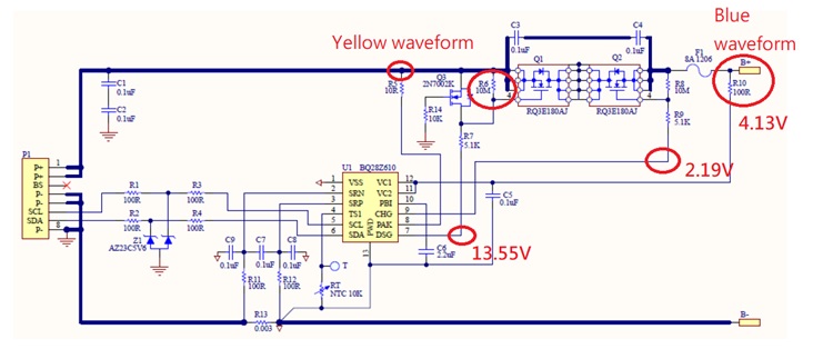
This thread has been locked.

If you have a related question, please click the "Ask a related question" button in the top right corner. The newly created question will be automatically linked to this question.

BQ28Z610: Pack+ have 5.7V ripple issue

Part Number: BQ28Z610

HI Sir 

Please kindly help to confirm why Pack+ have abnormal yellow waveform when the battery pack charge done 

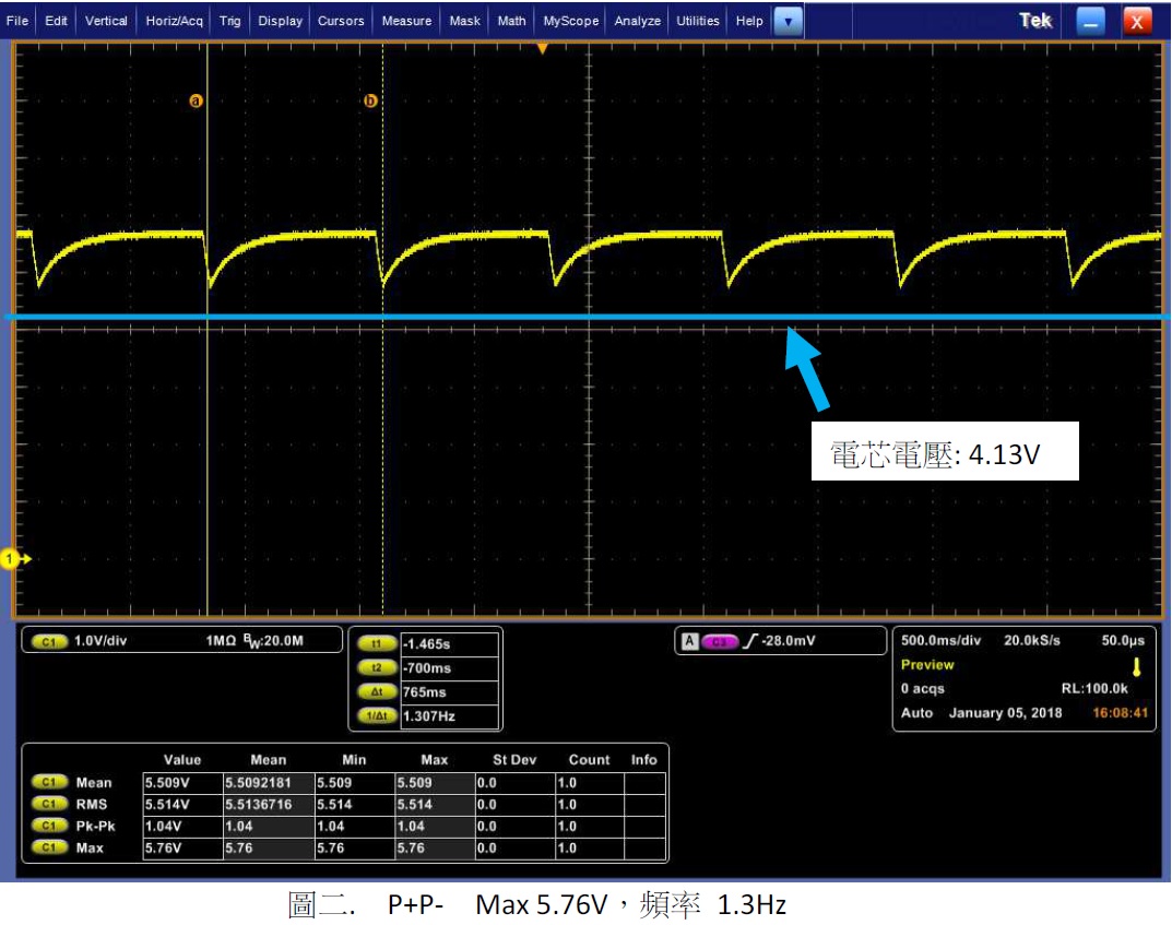
I think 5.7V ripple voltage is not correct on Pack+

Before remove R6

After remove R6

Pin7 DSG voltage (Remove R6 or without remove R6 ,the result is the same)

Pin9 CHG voltage (Remove R6 or without remove R6 ,the result is the same)

  • Hi Kai,

    Is the charger disabled at this point? The gauge has disabled the CHG FET to prevent further charging of the battery. Based on your plots it looks like the charger is still trying to charge the cell, but the gauge has disabled charging. The ripple appears to be from the charger. The charger need to be disabled  once charge termination is complete or set bq28z610 FET Options[CHGFET] = 0, which would keep the charge FET on even after charge termination is met. 

    See section 4.6 of the TRM (http://www.ti.com/lit/ug/sluua65b/sluua65b.pdf

    Valid Charge Termination The charge termination condition must be met to enable valid charge termination. The device has the following actions at charge termination, based on the flags settings:

    •  If FET Options[CHGFET] = 1 and GaugingStatus()[TC] = 1, CHG FET turns off. 
  • HI Damian

    In this condition Battery pack (BQ28Z610) doesn't connect with charger ==> Pack+ and Pack- floating

    We also remove R6 and only R5 connect this net ,but still have this waveform 

    May I know Pin8 PAK will effect this issue ?

  • Hi Kai,

    R5 is needed for pin 8 monitor PACK Voltage and to wake up device. Can you try applying a small load across PACK+ and PACK- and measure the PACK+ voltage with respect to PACK-. Leave R5 and R6 installed.

    You can also send FETEN command to enable the CHGFET then measure the PACK+ voltage with respect to PACK-.

    Please note that when the CHGFET Q2 is off as in this case the Voltage at PACK+ is most like coming from conduction through the body diode of CHGFET Q2.
  • HI Lewis 

    Thanks for your reply 

    "About this question ,our end customer worry this 5.7V will damage charger IC when we insert this fail battery pack to our tablet product" and end customer need us to explain this 5.7V will damage charger or not ?

    Do you have any idea how to setting this battery pack and will not have this 5.7V?

    When we add a external min load ,this 5.7V will change to battery voltage 


  • Hi Kai,

    I think this is similar to your other question. e2e.ti.com/.../2429326

    But I think it's because you have bad soldering on your dsg fet. Q1 might not be soldered down correctly.
  • Hi Kai,

    Batt is spot on. Please perform the following steps to test:

    1. Apply heat to the DSG FET (Q1) with a heat gun and monitor the ripple on the scope. As heat increases, the ripple should decrease.
    2. If so, please reflow your board.
    3. If the issue persists after reflowing your board, please log the event to and determine if the gauge is turning the FETS on or off. If the behavior appears unusual, please attach the log for further analysis.

    Sincerely,
    Bryan Kahler