


Other Parts Discussed in Thread: REF3433
Hi team,
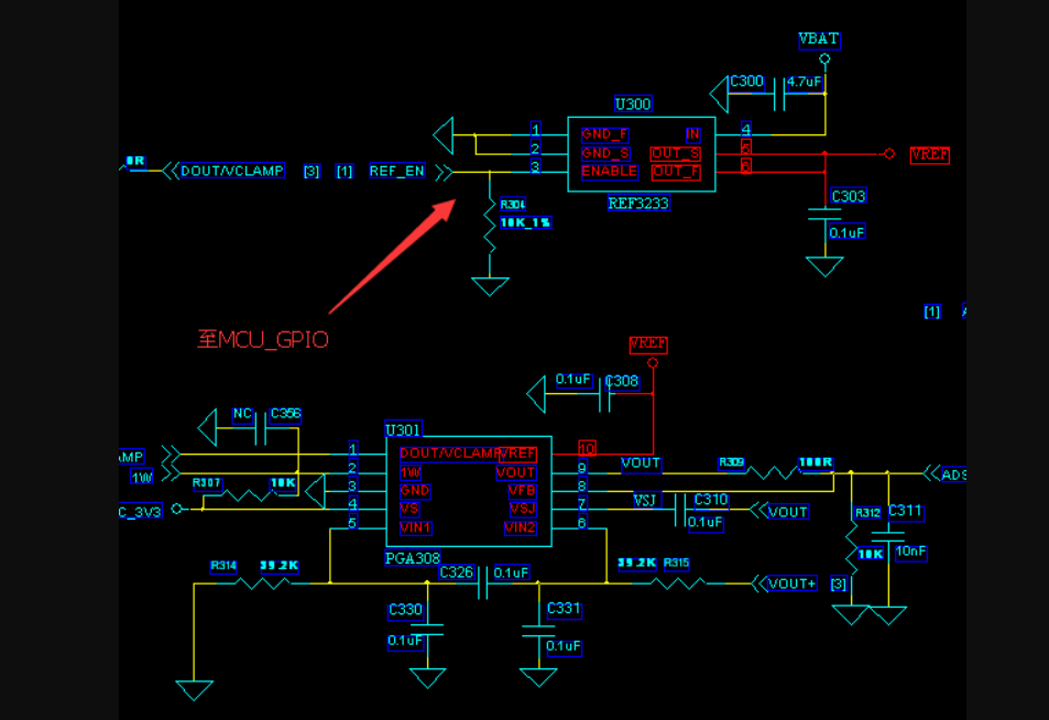
The customer uses REF3233. The attach is his schematic. The output voltage of REF3233 is connected to ADC.
The input voltage is 3.8V. The ENABLE pin is controlled by the GPIO of MCU. The GPIO pin can send a 3.3V
level voltage to the ENABLE pin.
When the output is no load, the output voltage is unstable. The output voltage can be 3.294V or 3.28V or 3.26V.
Would you explain this?
Best Wishes,
Mickey Zhang
Asia Customer Support Center
Texas Instruments


