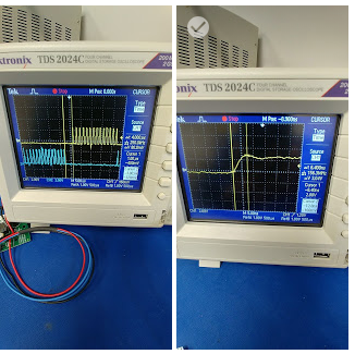
Hi I have schematic of customer prototype board that i can send . The PWM signals (3.3V) are coming from another eval board. HIN pulses 16 points for the first 25 uSec. 4 uSec later, LIN pulses another 16 points for the next 25 uSec. The 2 signals alternating continuously. The intend is to generate a sine wave at the test points 1 and 2. The B+ power supply is variable from 0 to 500 Vdc. At this time, I have D2, D3, D4, D5, D7, D8, D9, and D10 un-populated. He extracted this circuit from the schematic of the eval board UCC27714EVM-551. He expects the PWM signals to pass from HI to HO and LI to LO with some level of amplification (enough to switch on the FET). The PWM signals have the rise time of 6 nSec (see pictures below). The boot capacitor value and the diode come straight out of the datasheet. There are 2 electrolytic caps for the ICs. I can’t think you anything else I can do to get it to work. Please advise. Thank you
-
Ask a related question
What is a related question?A related question is a question created from another question. When the related question is created, it will be automatically linked to the original question.


