This thread has been locked.

If you have a related question, please click the "Ask a related question" button in the top right corner. The newly created question will be automatically linked to this question.

UCC28950 Constant Current / Constant Voltage with Automatic Crossover

Other Parts Discussed in Thread: UCC28950, TL431

Hi,

I want to use the UCC28950 in a battery charger design. I would like to have Constant Current / Constant Voltage with Automatic Crossover. This is typically done by "OR-ing" the voltage loop and current loop (error amps) with diodes.

Can I operate the UCC28950 with external error amp(s)?

Here is a good explanation of Constant Current / Constant Voltage with Automatic Crossover:

The category of DC power supplies discussed in this section changes AC line voltage into DC voltages. The most common and versatile regulated DC power supply is the constant current (CC) or constant voltage (CV) type which as the name implies can provide either a constant current or constant voltage within a certain range, see image below.

The working characteristic of this power supply is called a constant voltage/constant current automatic crossover type. This permits continuous transition from constant current to constant voltage modes in response to the load change. The intersection of constant voltage and constant current modes is called the crossover point. The figure below shows the relationship between this crossover point and the load.

For example, if the load is such that the power supply connected to it is operating in the constant voltage mode, a regulated output voltage is provided. The output voltage remains constant as the load increases, up until the point where the preset current limit is reached. At that point, the output current becomes constant and the output voltage drops in proportion to further increase in load. On some power supply models, the crossover point is indicated by a front panel LED indicators. The crossover point is reached when the CV indicator goes off and the CC indicator comes on.

Similarly, crossover from the constant current to the constant voltage mode automatically occurs from a decrease in load. A good example of this would be seen when charging a 12-volt battery. Initially, the open circuit voltage of the power supply may be preset for 13.8 volts. A low battery will place a heavy load on the supply and it will operate in the constant current mode, which may be adjusted for a 1 amp charging rate. As the battery becomes charged, and its voltage approaches 13.8 volts, its load decreases to the point where it no longer demands the full 1 amp charging rate. This is the crossover point where the power supply goes into the constant voltage mode.

Thanks,

Derek

  • Hi Derek

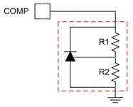
    Configure the UCC28950 to operate in peak current mode control. The error amplifier output voltage at the COMP pin corresponds to a current demand input to the current loop. Then limit the COMP pin so that it cannot exceed 2.5V. Then scale your external circuit so that this level corresponds to the current limit point you want to achieve. The controller will regulate the output voltage loop until the current demand (COMP pin) hits the limit at which point the system will operate in constant current mode. I've used a TL431 in the past to do this - it gives an accurate clean transition from constant V to constant I which isn't affected by temperature. The comp pin current will be limited to about 6.5ma when clamped in this manner. The current will come from VREF pin which has a short circuit current of 23mA (min) and it is designed to provide 10mA. So it depends on what is operating current (with switching) in the system. If operating current + 6.5mA > 10mA, then the 5V VREF may start drooping.

    the UCC28950 will go into a constant current mode if CS goes past 2V. This will then be followed by a hiccup mode of operation - you want to avoid that in your application - hence the external limit on the COMP pin.

    Regards

    Colin

  • Hi Colin,

    THANKS!!!

    I assume its OK to use the reference without a series resistor.

    Also, just for clarity, you show R1 and R2, but I assume I can just use the 2.495V.
    i.e. I don't need to make this EXACTLY 2.5V. Right?

    Thanks,
    Derek
  • Colin,

    One more question... Do I limit Vcomp BELOW 2.5V?

    I tried a 2.5V reference but the CS kicks in and the output hiccups. If I increase the slope comp (ME) by lowering Rsum, it doesn't hiccup but the crossover knee is very soft and the current increases as the load decreases.

    Thanks again!

    Derek

  • Hi Derek

    Using the shunt regulator with out a current limiting resistor is ok. The regulator will pull the right amount of current to regulate its ref terminal at 2.5v.

    2.5V isn't at all critical - I used it on the bench because it is easily obtained if you connect the regulator ref and cathodes together - probably ±5% would be fine. 

    The idea of clamping the COMP pin is to make sure that the switching cycle is terminated by the PWM COMP comparator and NOT by the Cycle-by-Cycle comparator. If the cycle-by-cycle comparator trips then the system enters hiccup mode. It's not shown in the block diagram but 850mV is added to the signal from the Ramp Summing block to the PWM COMP Comparator. This IS shown in Figure 37. If COMP is clamped at 2.5V then 1.65V (2.5V - 0.85V) should be the maximum signal level going into the cycle-by-cycle comparator which is less than the 2V level at its Non Inverting input and it should not trip. 

    Another - possibly better - approach is as follows.

    Remove the clamp on COMP.

    The controller will enter cycle-by-cycle current limit when the signal into the cycle-by-cycle comparator reaches 2V. (this signal is the CS signal plus the slope comp ramp of course)

    Defeat the entry in to Hiccup mode (refer to Figure 43). This can be done by using an ENABLE signal at the SS/EN pin with the following characteristics : High impedance at initial power up so that the controller can run through its soft start routine. It connects SS/EN pin to a voltage somewhere between VREF and 3.7V once the SS routine is complete, VREF will work. The SS/EN pin will pull up to the SS Clamp Voltage at the end of the SS time. If the controller enters cycle-by-cycle current limit the current into the SS/EN pin will increase, normally this will discharge the SS capacitor below the 3.6V OFF threshold. The purpose of the external ENABLE signal is to clamp the pin such that it does not fall below 3.6V - the system will remain in current limit indefinitely. I think that the external ENABLE signal could be generated by a simple comparator - even the TL431 with some resistors to set the threshold to 4.2V or so. Tie the TL431 cathode to the gate of a P MOSFET with its drain at VREF and source at SS/EN. I haven't worked out the details here but it should be simple enough and not expensive.

    The output current increasing as the load increases is a measure of the current regulation. There will be a voltage limit below which the current may increase significantly - largely due to minimum on times achievable in the power train. Anyhow - the system is regulating the signal into the cycle-by-cycle comparator. This signal is a composite of the slope compensation (which is necessary), the output current (scaled through the sensing network of course) and the transformer magnetizing current. Part of the regulation problem is likely to be due to the way that the peak to average signal varies with the duty cycle. The duty cycle will vary as the output voltage changes of course. take a look at the contribution to the CS signal due to the magnetizing current and see if you can increase the transformer magnetizing inductance or decrease the amount of output inductance.


    Regards
    Colin 


  • Hi Colin,

    Thanks again. First, I want to make sure I have the correct documentation. You reference figures 37 and 18. It appears (based on your comments) that these refer to Figures 12 and 18 (respectively) in the data sheet. Is there another document I should be reviewing?

    Based on your comments, clamping the SS/EN pin to 3.6V maximum will insure that the controller will not enter hiccup mode. You even said the controller “remains in current mode indefinitely”. Remember, I want CC and CV with automatic cross over. I am probably reading into your “Verbage” to deeply J.

    I am not sure I understand how the P-chan FET will achieve this clamping voltage. If the gate = ~4.2V, and the source = SS/EN pin and the drain = 5V, then the FET would be open until the SS/EN pin goes above 4.2V + Vgs(th)… i.e. >5.2V (for Vgs = 1V). I must be missing something… I usually do LOL. Can you explain further?  FYI, I don’t mind increased cost.

    Can I configure the internal error amp as a buffer and add two external error amps (one for voltage loop and one for current loop)? I have done this in the past with success but that was with a standard PWM. Basically, which ever “loop” is not in regulation would be at +5V and the diode would be reversed biased. The loop “IN” regulation would be between 0.8V – 2.8V (ramp) plus a diode drop. Here is the circuit I am suggesting:

     CV and CC Automatic Cross Over Circuit 25AUG2015.pdf

    Any and all help is very much appreciated!!!

    Again…. THANKS!

    Derek

  • Hi Mr.Colin and Derek,

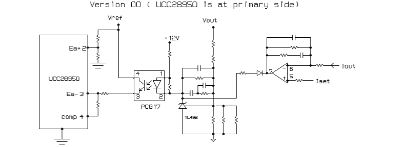
    I am using UCC28950 for the same purpose. In the earlier version, UCC28950 was at primary side and voltage and current feedback was given through TL431 as bellow. It is working well.   

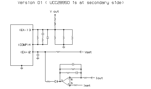
    In the revised version I placed the UCC28950 in secondary side. I am trying to take the voltage and current feedback as follows. 

    As per above configuration, when the unit went to CC it will try to reduce the CV set voltage.

    When the unit was in CV it's working fine but when it changed to CC I am observing the oscillations. Can we use above configuration for CC?. Please suggest if any changes required.

  • Hi Ashok

    I think you will need to change the schematic to connect the current amplifier output to the COMP pin rather than the EA+ pin.

    The reason is as follows. The new configuration will cascade the transfer functions of the current and voltage amplifiers and give you a really difficult compensation problem to solve. In the early version you connect the current amplifier output to the error amplifier output (TL431 Cathode) at the point marked with a red X so that the two transfer functions don't interfere with each other. You can modify your schematic to cut the connection at the red cross in the lower diagram and make the connection from the current amplifier to the COMP pin (green link).

    A few comments -

    You will have to study how best to make the connection and what the output voltage range of the current amplifier + diode will be. You may need to put in an active diode here - I'm not sure.

    You will have to compensate the current loop of course.

    Ideally this type of configuration is implemented using transconductance amplifiers but the error amplifier on the UCC28950 is a voltage amplifier. However, you should be able to make the circuit work.

    Regards
    Colin