This thread has been locked.

If you have a related question, please click the "Ask a related question" button in the top right corner. The newly created question will be automatically linked to this question.

UCC28951-Q1: Operating order of OUT pins

Part Number: UCC28951-Q1

Hello Application team,

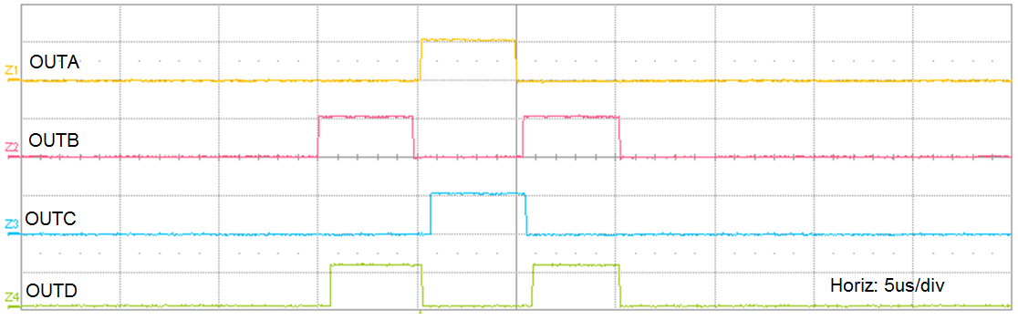
On DS page 8 of the data sheet "Figure 1, UCC28951-Q1 Startup Timing Diagram", It is expressed that OUTB first starts outputting.
Also in the "7.3.15 Synchronization (SYNC)" section and application report "SLUA 609", It seems that it is always output first from the output of OUTB.
Can we understand that the output of this IC is always controlled to start output from "OUTB" regardless of the slave mode?

Best regards,

Someno

  • Hello Someno-san

    You are correct, the OUTB pulse is always the first pulse out of the controller. The controller was developed to be compatible with external high side drivers. This sequence is necessary to allow the system to charge the bootstrap capacitor for the high side MOSFET QA before OUTA goes high. OUTD is delayed by TMIN from OUTB to allow charging of the bootstrap capacitor for the driver of QC.

    The screenshot below shows a typical pattern at Dmin.

    Regards
    Colin

  • I am getting similar pulses pattern. I am using external error amplifier while the internal error amplifier is configured as unity gain by shorting EA- and Comp pin. I am getting pulses at the output even when EA+ is connected to GND. Also, UCC28951-Q1 is going in Hiccup mode even if CS pin voltage is 0V. There is no change in min Duty cycle may be because the shortest duty cycle is set by the cycle-by-cycle current limit circuit, which becomes dominant over the duty cycle defined by the COMP pin voltage or by the TMIN block.
  • Hello Jignesh

    I'm not sure if you are asking for an explanation of this or not. Do remember that the UCC28951-Q1 can operate in Burst mode at light loads but it also can operate in a Hiccup mode at high currents. Even if you set the CS pin to zero voltage the PWM comparator will see the CS signal plus a ramp whose amplitude is set by the resistor at the RSUM pin.

    Please let me know if you need further clarification.
    Regards
    Colin