This thread has been locked.

If you have a related question, please click the "Ask a related question" button in the top right corner. The newly created question will be automatically linked to this question.

UCC28063A: UCC28063 IC Gate drive GDB "B" Output Failures

Part Number: UCC28063A
Other Parts Discussed in Thread: UCC28061,

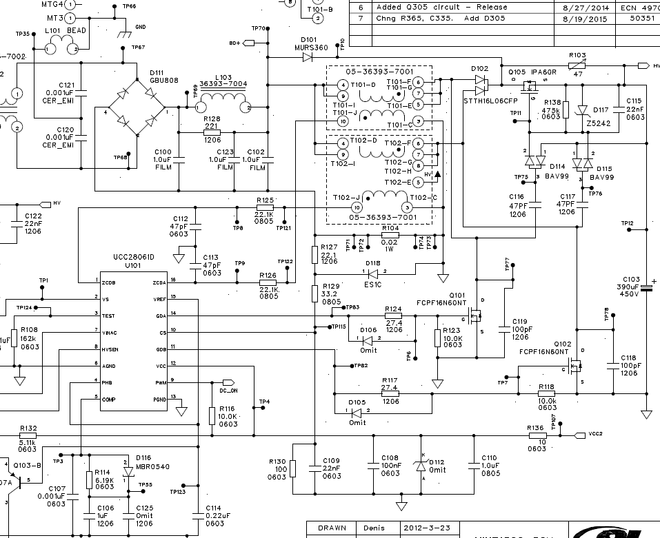
After updating from the older UCC28061 Interleaved PFC control IC to the newer "63A" version we have encountered failures of the "B" channel gate drive IC output.  The boost converter simply stops running and the boost voltage drop to the peak line voltage of about 325 from a 230 Vac line input. After inspection of the IC we find an internal low resistances of from 2-50 ohms from GDB pin 11 to Vcc pin 12. Some failures may also develop low resistance of 2-200 ohms from the Gnd pin 3 to GDB pin 11.  The GDA drive output shows no low resistance or signs of any stress. No other abnormalities appear on other pins of the IC or external components outside of the PFC converter control IC. The design has a 27.5 ohms series gate resistors on both the GDA and GDB gate drive outputs to the boost FET's. After the PFC control IC is replaced the power supply fuctions normally. The Controller is powered from a 13.4 VDC auxiliary power supply, runs at 70 kHz under full load and is capable of delivering 400VDC at 500W.

Is there any known history of gate driver "B" output failing in this manner ?

John  

  • Hello John,

    You do not say if you made any changes to your circuit for this change. Did you simply replace the UCC28061 with the UCC28063A ?
    I understand that GDB fails but it also seems that GDA is turning off or fails since the pfc output is not reaching the set value.

    Attached is a document showing the differences between both of these parts and you can see that most of the differences relate to the error amplifier.

    0184.Differences UCC28063 and UCC28061.pptx

    There should be no difference relating to the gate drive and there is no "history" of gate drive B issues.

    I think there is something going on in your design and you should try and capture some switching waveforms of the gate drive.

    If you attach a pdf of the schematic then I can review and offer suggestions.

    Regards

    John


  • Hi John -

    We have replaced the UCC28061 directly with UCC28063A with no circuit changes to our current design.

    Units run during our production testing and the PFC simply stops boosting to 400 VDC and our DC converter shuts down due to low DC +Bus condition.

    No other components are damaged outside of the “63A”. The DC Bias supply is not overloaded but the unit has no gate drive output on either GDB or GDB drive pins.  All other parameters look OK.

    Doing a simple resistance check shows the GDB has very low resistance back to Vcc and sometimes the Gnd pin also. GDA drive output pin looks OK and shows no low resistance.

    Once the PFC controller is replaced the units run normally.

    Our reference schematic shows the PFC design with the “61” referenced but the “63A’ is actually installed instead.

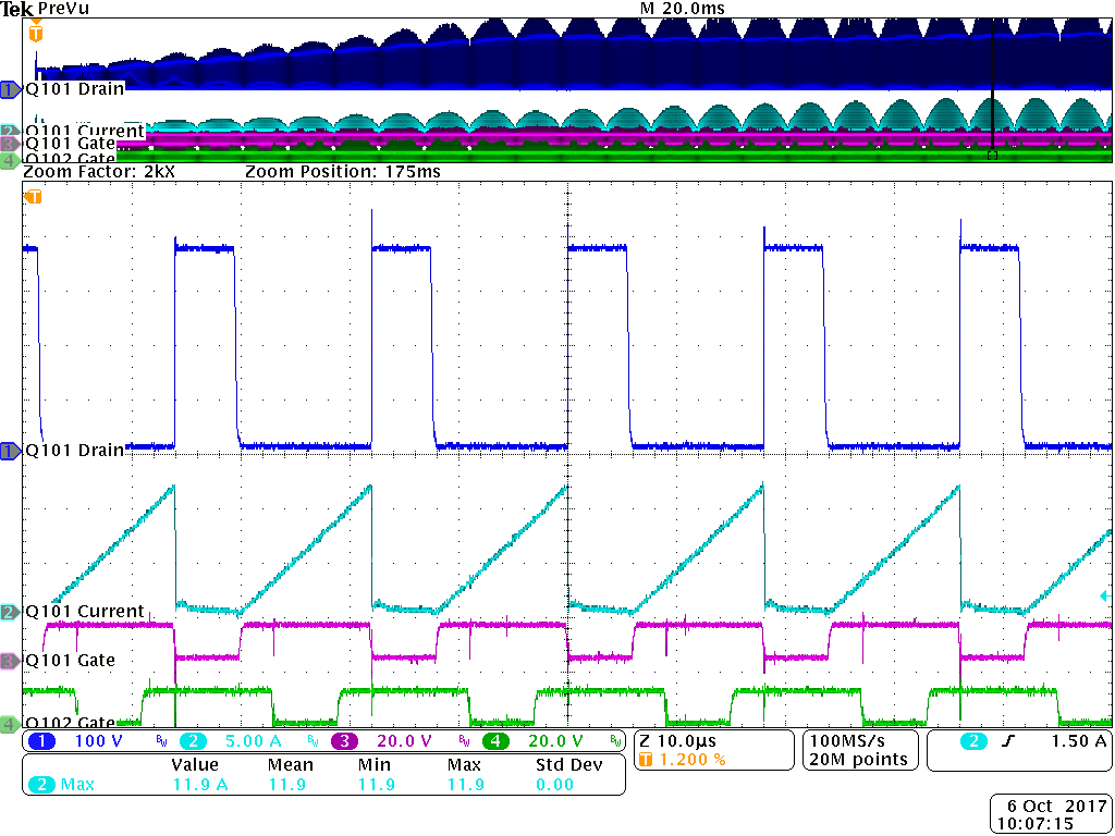
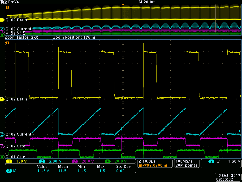
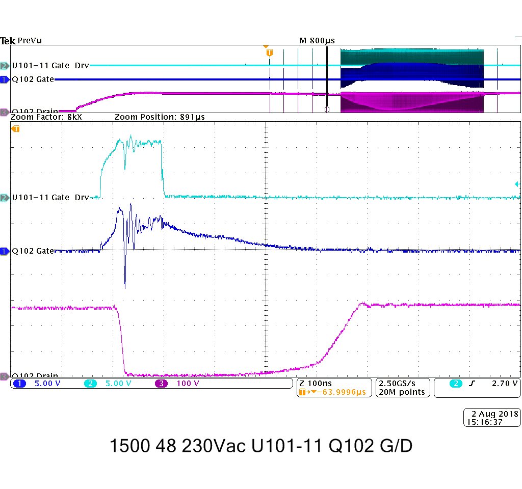
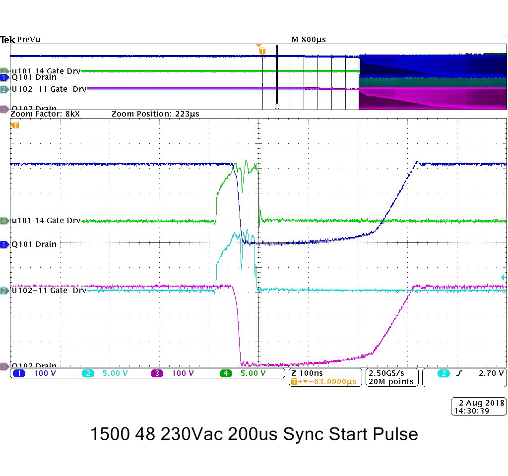
    I have also attached scope shots of the gate drives during the prestart 200uS gate pulses and during a loaded boost operation.

    We were concerned about the 200uS start up event and if the amplitude of the switching of the FET ON could stress the “63A” gate drives negative voltage limit of -0.5 volts. We have not captured this but the 180 nS or less gate drive amplitude just turns the FET’s on and the active gate capacitance is at it’s worst and couples the drain switching edge back into the output driver to some extent.  Could this be an issue ? MOS FET Coss increases as the source drain voltage drops.  The fast edge couples this back into the gate drive output through the 27.4 ohm gate drive resistors R117 and R124.  This appears to be approximately 500mA of current during the turn on drain falling edge transition.  What are your thoughts on this aspect ? Could this condition damage just “B” side gate drive output section ? It seems to have the highest amplitude of the two gate drive signals with our PCB the layout.

    We appreciate your quick response to our post.

    Thanks,

    john

  •  Additional wave

    a

    Additional waveforms-

  • Hello John,

    Thanks for sending the additional information.
    The schematic is drawn for a current limit set at 15A with the components values shown.
    You dont specify what power level is used in this application but 15A is a very high current limit and I wonder if it is set too high.
    With the limit set too high there is a danger that the pfc is switching during the current inrush and this can lead to boost MOSFET failure.
    I also notice that the inrush limiter R103 is an unusual arrangement in series with the output capacitance and is not in part of the boost MOSFETs.
    So my suspicion is that there is some issue during startup.

    I recommend that you run the Excel calculator tool for the UCC28063A and increase the value of R104 from 20mOhms.

    Also failure of the GDB or GDA output is generally associated with ringing on the output. This can be eliminated by placing reverse diodes from GDA/GDB to ground and from GDA/GDB to VCC.
    I dont see anything else in the schematic or the wave forms you attached but I would also recommend that you look at the pcb layout and see if there is anything unusual about the routing associated with the GDB trace.

    Hope this helps with your troubleshooting.

    Regards

    John

  • Hello John (G) -

    The PFC converter supplies 400VDC at 550W to maintain a 500 watts of DC output power. We have not encountered FET failures during powering up or at 120% overload operating conditions. Startup appears to be very stable using the "63A". 

    The earlier design used the UCC28061 and the same PCB and did not suffer the GDB output driver failures.  We have not observed any ringing at either of the GDA or GDB output pins of the "63A". We do see the GDA and GDB voltage drop while the FET turning "ON". This occurs during the 200uS  restart timer before the boost soft start and during light loading.

    Our main focus is the gate output spike as the FET turns on. As the FET drain voltage falls (11 nS fall time) to approx. 50-100 volts,  Coss of the FET increases dramatically. This is coupling through the series 27.4 ohm and loads the GDB output down. The additional loading pulls the GDB pin down about 5 volts in the reference shot implying that about 180 mA's current is being sourced out of the GDB pin. 

    If the FET gate were to drop below ground and become negative could the output driver circuitry become permanently damaged ?

    Any issues running the "63A" at 13.4 VDC ?

    Any issue with increasing the gate series resistor to 75 - 100 ohms to further attenuate the effects of Coss and the fast turn on edge of the FET's ?

    I will review the layout on both the GDA and GDB circuits and the diode clamp opposition.

    John


  • Hello John,

    If your converter is drawing 500W of power then you will need a gate driver to interface the controller to the MOSFETs.

    This is regardless of whether you use the UCC28061 or the UCC28063A . You can use a integrated ic gate driver or you can use the simple totem pole driver as shown in the attached sketch. 

    2364.driver.pdf

    The UCC28061 and the UCC28063A both have a maximum UVLO threshold of 13.5V so 13.4V on VCC will not always  power up either of these ic's.
    A supply voltage of say 14V or 15V is guaranteed to power up the ic's.

    Regards

    John

  • Hi John,

    Thank you  for the gate driver circuit reference details. We have used it in the past in various designs. 

    What is the basis for an additional external gate driver over of the "63A" own internal gate driver ?

    The FET's we are currently using have a specified Coss of approximately 1500 pF as the drain passes 100 VDC and that continues to increases to about 4000 pF as the gate transitions below 10 VDC during  turn on.

    Is there a maximum capacitive load limit on the current internal diver? Your app note shows testing with 4700 pF of capacitance on the GDX outputs.

    Do you feel this could present a problem for the internal gate drive output ?

    We will review the Vcc bias set point as you have noted.

    Can I contact you directly and talk over the driver failures we are seeing ?

    Thanks,

    John

  • Hi John,

    You can contact me at johngriffin@ti.com if you need further help.

    Regards

    John

  • Hi John,
    I am goin to close this post since the question is being addressed by email.
    Regards
    John
  • OK - Appreciate the support

    Thank You