A related question is a question created from another question. When the related question is created, it will be automatically linked to the original question.
If you have a related question, please click the "Ask a related question" button in the top right corner. The newly created question will be automatically linked to this question.
I had looked at this device also based on your earlier query. But this does not have the fourth rail (DVDD) that TPS65105 had with the LDO controller. Would your system provide DVDD separately? If three rails will work for your application then let me look into the timing of this device and I will get back to you.
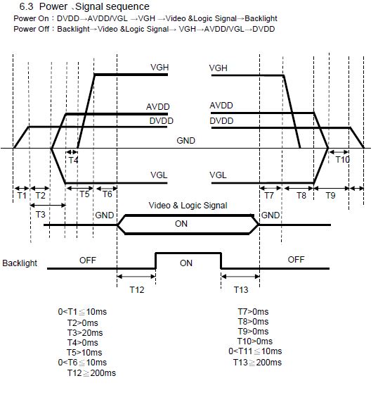
I reviewed TPS65150 power sequencing and your LCD panel timing diagram and below is what I have been able to infer.
T1 -- is independent of TPS65150 as DVDD will be provided by your system
T2 & T3 -- is independent of TPS65150 as your system will provide the input voltage to TPS65150 and should time it such that power to TPS65150 is not provided until DVDD has been stable for atleast 20ms.
T4 & T5 -- choose Cdly1 of very small value (like 10pf) and Cdly2 of ~47nF to provide a delay ~11ms for T5. Please see section 7.3.4 on page 17 of datasheet for further details on calculating delay times.
T6 -- is independent of TPS65150 as video output will be controlled by TCON/your system.
T7 & T8 & T9 & T10 --- are independent of TPS65150 as input supply to TPS65150 and DVDD supply will be controlled by your system.
T11 -- I do not know what this time is as I could not find it in the timing diagram.
T12 &T13 -- are independent of TPS65150 and will controlled by back light controller.
Hello Nishmitha,
The amount of input current depends on the output voltage of the boost converter, charge pumps and load current. Basically, it is conversion of power with some loss so input power (Vin*Iin)= Pout/efficiency. Generally , the lower the conversion ratio (Vout/Vin), the better the efficiency. So Iin will be higher for 3.3V compared to 5V but how much will it be will depend on the Vvs, Vgl and Vgh output voltages and load currents for each output. Please take a look at figures 18, 19 and 20 in the datasheet which show boost efficiency at various input voltages, output voltages and load current levels.
Kind Regards,
Liaqat
Hello Nishmitha,
Since boost output powers positive charge pump, negative charge pump and VCOM through the SUP pin, you have to consider boost output current as sum of current going into SUP pin + any other load on boost output and calculate Iin accordingly. As a rough approximation (since there is no efficiency information in the datasheet about the charge pumps), I would suggest to consider charge pump power conversion efficiencies at 70%.
Kind Regards,
Liaqat
I have one more query regarding the timing setting.
1) Is it possible to achieve VGH voltage before VGL .
2) Is it possible to set DLYI pin delay to 0ms to achieve AVDD and VGH at the same time. If its possible what would be the possible connectioncat DLY1.
Hello Nishmitha,
It is not possible to achieve VGH before VGL as VGH does not start until VGL is valid.
DLY1 delay is between AVDD valid to when VGL starts up. So DLY1 does not control the delay between AVDD and VGH. As I mentioned above, VGH will not start until VGL is valid.