This thread has been locked.

If you have a related question, please click the "Ask a related question" button in the top right corner. The newly created question will be automatically linked to this question.

TPS7A7001: question about polling time

Part Number: TPS7A7001
Other Parts Discussed in Thread: TPS7A7002, TPS7A92

Hi,

Ask about TPS7A7001/002 polling time.
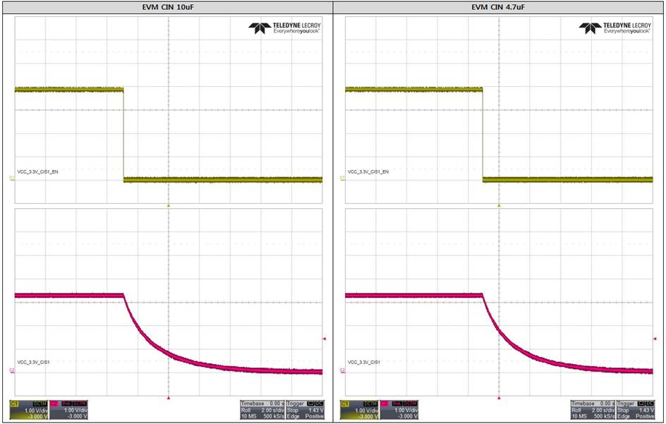
If power is removed from the EN pin through our board, it takes about 20 seconds for Vout to reach 0V.
It takes about 10 seconds to check through TI EVM.

When tested with EVM, the input and output capacitors used the default devices.

Below is the environment that is applied to our board.
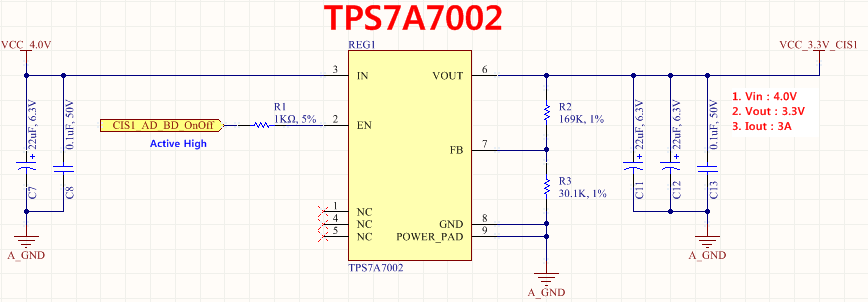
Vin Vout Iout device remark
5V 4V 2A TPS7A7001 2pcs
2V 1.1V 3A TPS7A7002 2pcs
3.3V 2.5V 2A TPS7A7001
2.5V 1.35V 2A TPS7A7001
4V 3.3V 3A TPS7A7002 2pcs


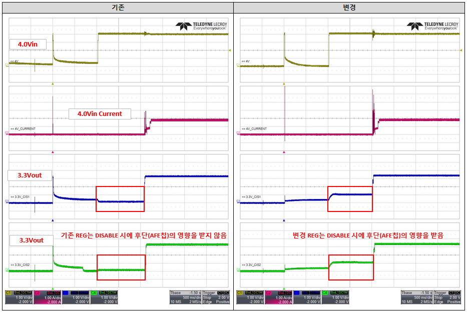
In addition, the following waveforms were taken from our board and TI EVM.
CH1 : EN / CH2 : Vout
1> our board (5sec Time/Div)
2> TI EVM (2sec Time/Div)

Please let me know if the polling time is originally this long, or if there is a way to improve it.

In addition, I'd like to hear your opinion to use tantal capacitors as input and output capacitors.
Tantal has better temp sensitivity spec rather than ceramics.

thanks,

TS

  • Hi TS,

    TPS7A7001 does not have active discharging from the LDO itself. When being disabled from enable pin, Vout can only be charged through resistor dividers parth to ground, leakage and the load you have.

    Based on the information you provided, you have current load ranging from 2A to 3A. I can also see that you have tried to show discharging curves with different output caps. If we have 2A load taking current out from Vout pin, with a 10uF cap initially holding a 4V voltage potential, the discharging time from 4V to 0V should be t = 10uF x 4V / 2A = 20us.

    The plot you showed gives me a feeling that there is no 2A or 3A load on the Vout while curves being taken. If there is no active load for discharging, Vout will be primarily charged through resistors dividers and through capacitor leakage. The discharging timing constant can be estimated as RxC; if you are using 10uF cap and have a 30KOhms (R1+R2) on your boards, the timing constant is 0.3 seconds. It could take 1.5 seconds for Vout to fully discharged. If your discharging time seems to be extremely long, please double check the resistors you used. If the resistance value increased to 300KOhms, with 10uF output cap, the discharging time could take up to 15 seconds.

    Regards,
    Jason Song

  • Hi Jason,

    thanks for your quick answer.

    In case of TPS7A7001/2 LDO, it is stated that R2 resistor value should be selected between 27 ~ 33K.

    Is it not possible to say that it is lowered to about 30K based on R1 + R2?

    If we simply select the resistor value ratio, we can set it to 30K (R1 + R2), but it is impossible if you follow the specifications from the datasheet below.

    Please check for this.

    thanks,

    TS

  • In the case of the transmitted waveform above, it is at no load.

    The waveform on load seems to be OK.
  • Hi TS,

    Can you share with me the resistor values you used in your resistor divider for your output versions?

    Regards,
    Jason Song
  • Hi jason,

    Schematic and issue as below.
    There are two major issues.
    Both issues are not a problem when using DIODES products before.
    1. Maintain Voltage in LDO Disable State
    2. LDO Enable Pin Difference between current consumption and output voltage variation in PWM control

    Waveform
    1) Comparison of operating waveform before and after change
     Keep voltage in LDO Disable state (existing(DIODES): no output / change(TI): 1V voltage maintenance)
     Test condition: Measurement under the same conditions except LDO peripheral circuits

    2) On / off PWM control causes difference in current consumption
     LDO Enable Pin Difference in current consumption and output voltage fluctuation during PWM control

    thanks,

    TS

  • Hi TS,

    In the waveform you attached, from top to bottom: Vin(voltage in yellow), Vin(current in pink), ???(in blue) an ???(in green). It seems to me that blue one is enable and green one is Vout. Is that right?

    Regards,
    Jason Song
  • Hi Jason,

    I added the description to the waveform below.
    thanks,
    TS
  • Hi TS,

    Thanks for the clarification.
    In order to better assist with your issues, I have a few questions to ask regarding to the two items you listed

    1) Comparison of operating waveform before and after change
    a. Can you provide the waveform and show when Enable signal has been provided?
    b. What else you have on your output pin? it seems to be you may have other leakage from your circuitry that source current through the resistors divider and bring up the voltage to 1V.
    c. Can you provide the part number from DIODES? Their device seems to have a strong pull down. Our device has no pull down circuitry and the vout pin is being discharged only through loads.

    2) On / off PWM control causes difference in current consumption
    This LDO is not designed for application with PWM. May I know what is the application for this PWM? What's your objective?

    Regards,
    Jason Song
  • Hi Jason,

    The part name of DIODE is  AP7176BSP-13.

    Basically AFE(Analog Front End chip for sensor) was connected with Output pin of TPS7A7002 and need to check other device is also connected.

    Will update other questions soon.

    Do you think there is no problem in schematic (Especially resistor value)?

    There is mismatching between your comment and datasheet above and we didn't get the answer for right value of resistor yet.

    I also think the resistor value have some point to solve this issue.

  • Hi TS,

    According to the datasheet, the resistors values you picked are fine. The reason I asked you to reduce the size of the resistors is to address the slow discharging you mentioned at your first post. As this device does not have active discharging circuit and the slow discharging you have seen without load does make sense based on our estimation. Reducing the values for the R1 and R2 will increase the quiescent current consumption, datasheet is trying to give you guidance on the resistors value that will minimize the quiescent current.

    Does it make sense?

    Regards,
    Jason Song
  • Hi Jason,

    TS(Disty FAE) is in business travel in Dallas this week. so pls refer to below comments.

    Yes i think the resistor value is not key factor to make output voltage to 1V after disable EN pin.

    we tested adding addition load resistor (1K-10Kohm) to make the 1V to 0V but the output was still 1V.

    We also found similar issue & this method(adding load resistor) in other customer thru Forum.

    Pls give us other solution by today if possible,

    According to customer, if we can't give solution by tomorrow, customer will change the solution to competitor.


    For your question in the previous message,

    1)I think EN timing is not cause for this problem and there is only AFE chip(analog front End) for sensors.

    2) PWM is input for EN pin to control on/off of LDO. Is there any problem?
  • Hi Danny,

    The schematic looks okay. The resistors you currently have in the circuit are good too according to the recommendation on the datasheet. The main reason for the residue voltage on the Vout when device is disabled is due to the fact that this device has no active pull down circuit. We would recommend using TPS7A92 with active pull down circuit if the residue voltage is a concern for the application.

    There are multiple reason that could cause the residue voltage on the Vout even when device has been disabled by pulling down Enable. One reason is due to the leakage from the internal pass device. Even when the pass FET device has been shut off, there is still leakage from the device that could pull Vout up with the small leakage being built up on the resistor divider. Other reason could be related with external circuitry that has shared the Vout pin; when you have other devices connected to the Vout pin, it could have leakage as well. With the resistors you have in the schematic, with 200K OHms resistance existed on the Vout, a 5-uA leakage could bring Vout to somewhere close to 1V. Since I have noticed several forum posts reporting similar concern over the residue voltage, I am setting up an bench to run some evaluation to see how big the leakage could be. I have studied the TPS7A7002 EVM on bench and with the resistors on the EVM which is 30KOhms, I am seeing little residue voltage. That's why I am suggesting you to reduce the resistance to ground, you could do this by reducing the resistor divider value or apply additional load that will be a load in parallel with the current. If you add another 1K Ohms resistor, the vout residue will be negligible. Please try it and let us know.

    For your questions regarding the PWM, usually when you mention PWM, it refers to using clock duty cycle to control the output high and low duration. Since the discharging of this device is extremely slow, it does not make sense to use this device with any PWM related application. Like I mentioned, you should consider using TPS7A92 which has the active pull down circuitry for fast discharging to PWM related applications.

    Regards,
    Jason Song