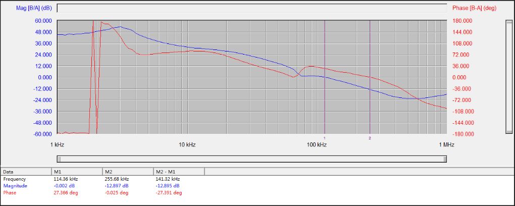
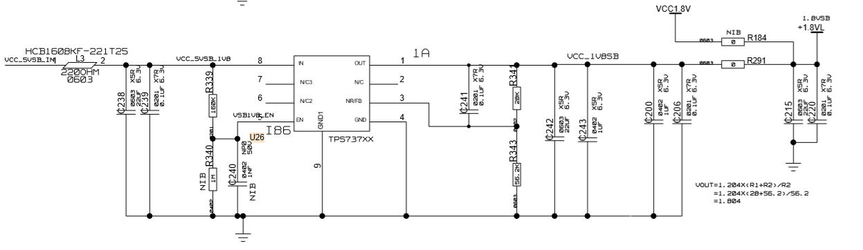
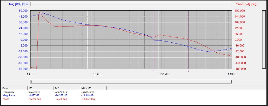
TPS73701 Schematic diagram is below.Test Phase and Gain Margin by removed C241,the Phase value is less than 30° when loading is 0.25A or 0A;the phase is greater than 30° when loadind is 0.5A.How can I optimize the design to ensure the phase value is greater than 30°.Please give me some suggestion,thanks!
The Schematic diagram:
The Bode diagram under 0A loading:
The Bode diagram under 0.25A loading: