This thread has been locked.

If you have a related question, please click the "Ask a related question" button in the top right corner. The newly created question will be automatically linked to this question.

tps62260's failing

Other Parts Discussed in Thread: TPS62260, TPS23750, TPS54218, TPS62240, TPS63020, TPS62750

I keep killing TPS62260 regulators, but I for the life of me, I can't figure out how or why.

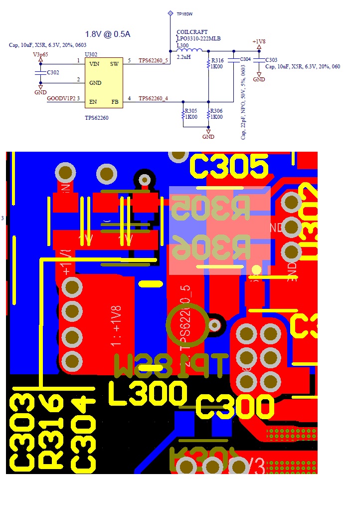
The tps62260 regulator provides the 1.8V supply for a DaVinci DM6446 design, regulating down from a 3.65 volt rail coming from a TPS23750 POE design. See attached picture.

I used to have fairly high impedance resistors in the feedback network, but found that just touching the leads on the devices with my finger would cause some evil to happen that resulted in the devices getting excessively hot, and destroyed. So I lowered the impedance of the sense node dramatically.

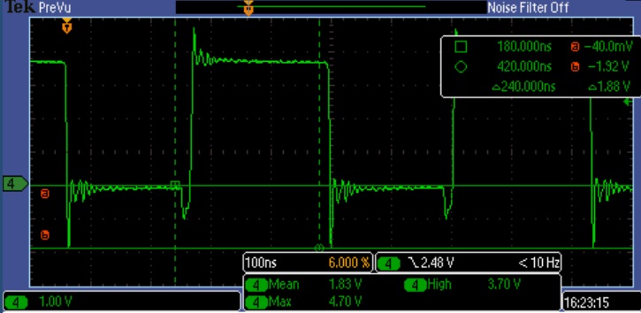
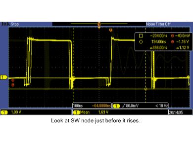
The load on the device is not excessive, just two drams and the 6446 itself. The input power seems pretty clean. Yet, for reasons unknown, these devices continue to fail in the field. One I am looking at now just doesn't try to switch. Actually both the switch node and the output is just sitting at about 350 mV. The input, and the enable are both at 3.65 volts.

The part that really has me confused is that these devices are supposed to both be thermally and overcurrent protected. These boards are coming off a production line (not some hand soldering with questionable static control). The board is 6 layers and emedded within casework which has been ESD tested. If we are damaging the parts, I can't see how.

Would excessive capacitance on the output lines explain such an issue? There is well over 100uF on the line spread over the board area feeding the Davinci, the DDR, and a couple of other small places (level shifters, etc).

Hedley

  • Yes, you have placed too much output capacitance on the output, thereby making the part unstable.  My guess is that when the load on its output changes--which happens very frequently and very fast in your application--the part oscillates and overshoots a lot causing the voltage on the SW pin to exceed the maximum rating.  This destroys the part.  The allowable output cap range is given on page 19.  You have exceeded the maximum allowed 22uF by at least 5x.

    With these internally compensated parts, you must use the recommended L and Cout for stability.  To get this IC to work, you need to lower the output cap to 22uF.  If you need to support that much, you will need to use a different part, such as a TPS54218, which has external compensation.

    Yes, the FB pin is sensitive to noise and other signals especially the capacitance of your finger.  If the user could touch the circuit in the end application, then you need to lower the divider resistance like you did.

    Thank you for posting your schematic and layout.  Both look good.

    Are you sure all that stuff this powers will draw less than the 600 mA it is rated for?  The device will protect itself in an overload, but you need to size your power supply to handle the peak current demand.

  • Are you sure all that stuff this powers will draw less than the 600 mA it is rated for?  Depends on who you can trust. I powered this rail from a bench supply, and according to both it and a separate multimeter, the actual average current draw is about 250mA. Besides, its not thermal shutdowns that I am seeing, after all, they would self repair.

    I ripped caps off of the board, and am now down to something like 17uF total on the entire board, 10 of which is the output cap for the regulator. The system appears to be running, although this will need some serious qual work.

    Lets talk about that SW pin. It is pretty darn ugly, 1.8V of undershoot, and maybe 1V of overshoot. Scope shot attached.. The Absolute Max Ratings say -0.3V to 7.0V for the SW pin. If the layout is okay, and the schematic is okay, how do I reconcile the undershoot vs. the absolute maximum rating for the part?

  • This undershoot is ok as it is at the point where the high side FET turns off and the low side FET turns on.  There is dead time there in which neither FET is on.  But the inductor current must still circulate.  It does so through the low side FET body diode.  Thus, the higher drop.  If you probe the SW pin to the GND of the IC with a low inductance probe--wire wrap around the ground barrel, not the clip lead--this will look less as you will pick up less noise and have less inductance in the measurement.  Same thing on the overshoot.

    Your layout could be improved by moving the input cap where those 3 vias are, so it is right next to the pins and moving the output cap closer so that its ground is nearer pin 2 than it is now.  But you shouldn't be destroying anything due to your layout the way it is now.

  • This shot was taken with the scope probe above probing directly on the pins of the TPS62260. Yes my previous scope technique was sloppy, but still, there is an issue here. 1.1V of undershoot, and a pretty good chunk of 0.7 or 0.8 volts just before the SW node rises.

    The Absolute Max Ratings say -0.3V to 7.0V for the SW pin. If the layout is okay, and the schematic is okay, (and my cheesy scope technique is okay), how do I reconcile the undershoot vs. the absolute maximum rating for the part?


  • Yes, this undershoot is ok.  The -0.3V rating simply informs the user that there is a diode there.  There is a body diode on the low side FET that will conduct for a brief period after the high side FET turns off and before the low side FET turns on.  It must conduct and it has a voltage drop in excess of 0.3V.  This isn't a problem.

  • The datasheet of the TPS62260 and TPS62240 state:

    For stable operation, the L and C values of the output filter may not fall below 1μH effective Inductance and 3.5μF effective capacitance. Selecting larger capacitors is less critical because the corner frequency of the L-C filter moves to lower frequencies with fewer stability problems.

    This statement is technically fully correct. I also have an app, where a GSM module needs quite huge capacitive supply buffering. Even when I load the output with a fixed resistor, such that approx. 60% of full load is reached, instabilities in the output supply voltage are obeyable.

    If Chris' statement still holds, the datasheet(s) must be corrected. That would avoid situations where engineers choose products for prototypes that will fail finally.

  • The TPS62260 D/S does not have the last sentence in that paragraph.

    For your application, the TPS63020 is often used or possibly the TPS62750 which is designed to support large output caps.

  • Hm, sorry, you're right with this. A slight difference which I overlooked. Some experiences seem to confirm that the TPS62240 is stable when loaded with big caps (totals up to approx. 500 uF), while the TPS62260 tends to slightly oscillate around 20 kHz.

    The alternative devices mentioned are too expensive and or too big max. current. Meanwhile I have selected a current mode regulator (ST1S12XX), since they are easier kept stable.

  • Are you sure you want to use an IC that has such a sparse datasheet?  Being internally compensated (even though it is current mode control) means it also has a range of stable output filters.  The difference is, that with that part as opposed to the TPS62260, they don't tell you what that range is!  (do they have a forum to ask this on?)

    Your local FAE can help you select the right TI part for your specific application.

  • Independently of your feedback, I got to a datasheet of NCP1521B (also current mode), which SOT23-5 package is even pin compatible to TPS62240/60. I'll get samples of it.