This thread has been locked.

If you have a related question, please click the "Ask a related question" button in the top right corner. The newly created question will be automatically linked to this question.

Boost converter with true disconnection between Vin and Vout

Other Parts Discussed in Thread: TPS61088, TPS61093, TPS61085

Hi Everyone,

Our customer is looking for boost converter with true disconnection between Vin and Vout that can meet following requirement.

  • Vin = 2.8V to 4.2V
  • Vout = 10V
  • Iout = 0.3A

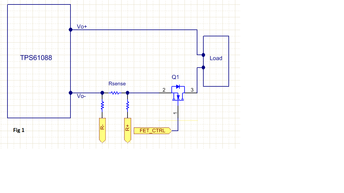
I found that TPS61088 is synchronous boost converter so it looks nice but I believe that it can not disconnect between Vin and Vout...

Please let me know if you have good solution to meet this requirement.

Best Regards,

Sonoki

  • SonokiIf this peak current is lower than 1.1A, then TPS61093 is a good choice.
    But in this application, at the minimum input voltage, the input current is about 1.2A, so the peak switch current will be higher than 1.2A. So TPS61085 is a good choice. It is much cheaper than TPS61088.
    But you need add a MOSFET at the return ground. So the TPS61085 and the MOSFET be disabled and enabled at the sametime. And at the output short circuit condition, by detecting the output voltage or output current, the MOSFET can also be disabled in those conditions.
    BR,Helen
  • Sonoki,
    Could you please share the detailed application information for us? Like in what kind of equipment? Volume? MP schdule?
    My email address is helen-chen@ti.com Thanks,Helen
  • Hi Helen,

    Thank you for your comment. I'll contact you directly.

    Best Regards,

    Sonoki

  • Looking at the block diagram for the TPS61093, I'm curious how the dc path is eliminated VIN > VOUT?  L1 is connected between VIN and SW, then there is a forward-biased diode from SW to VO.  From VO to VOUT, a FET, and the body diode will allow dc to be present at VOUT, correct?

    Compared to the block diagram for the TPS61088, L1 is connected between VIN and SW, SW FET to VOUT.  Basically the same as the TPS61093 except the diode is missing.  In both cases, if  VIN is present, it will appear at VOUT.  What seems to be different with the TPS61093 is that if VOUT is present, it will NOT appear at VIN, if VIN is disconnected or OFF.

    I do need an isolated, or, simply a design where VIN will not appear at VOUT when the converter is not ENabled.  3-4VIN, 6VOUT at 3A.  Any suggestions?

    ~Leonard 

        . 

  • Leonard
    about the TPS61093, the internal diode direction is from VOUT to VO, so it will isolate the VIN from VOUT when the device is disable.

    we don't have a one device solution for 3-4V, 6V@3A currently. we can add a external isolated FET between TPS61088 and the load, as TPS61093
    May i know the application field and potential volume of this kind of application.
  • Hi Leonard,


    I also post my reply here in case more person can see the answer:


    TPS61088 doesn’t has load disconnect function. The customer need to add an extra MOSFET at the output side. This MOSFET can be used for both load disconnect and short circuit function. Please check the below picture:

    1. when output is shorted, the ouput voltage will be low, and the output current will be very high.  Suggest the customer to detect the output voltage or the output current (use a sense resistor Rsense) by a MCU, if the output voltage is lower than a certain value or the output current is higher than a certain value,  turn-off Q1.

    2. Enable/disable the MOSFET and the TPS61088 at the same time to realize the load disconnect function.


    Thanks!


    Best regards,

    Helen

  • Here's the simplified schematic:

  • If we don't want to monitor the current, we can eliminate Rsense, and simply disconnect the RTN of the load; the TPS61088 already has a ILimit function.  However, I'm wondering how practical this is to open the GND path, as most GND connections are to a GND plane, plus the TPS61088 has a GND power pad.

    Would it not be easier to put the FET directly at the VOUT pin?  Even so, at high currents, this has to feed a large power plane. 

    The other aspect of this suggested approach is the load is not a single device, it is dozens of other ICs, maybe an FPGA or Processor, so it becomes rather impractical to implement the FET in the GND path.

    Do we have another approach that would isolate the VOUT path?

    ~Leonard

        .

  • Then you can add a PMOS at VOUT+.  I reply you in the email :)