This thread has been locked.

If you have a related question, please click the "Ask a related question" button in the top right corner. The newly created question will be automatically linked to this question.

TPS62160 Design Review?

Other Parts Discussed in Thread: TPS62160-Q1

Hello,

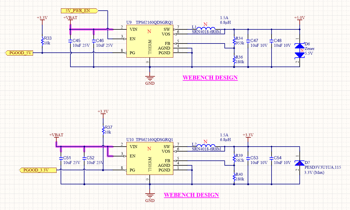
We're in the process of designing our new electronics and have decided to go with the TPS62160-Q1 for our power supplies; 3.3V  and 5V. We went with a larger inductor and output capacitor in order to reduce the output voltage ripple to <1mv. The combination isn't in the recommended components and isn't listed in the loop stability table (http://www.ti.com/lit/an/slva463a/slva463a.pdf

I've posted our schematic and pcb below. We gave a global +3.3V plane and the VOS input for the 3.3V DC/DC  is connected to this plane, as opposed to a single trace (as it's done for the 5V). Could this cause any issues? I'm also unsure about the GND vias. We're trying to keep a single point of entry in order to minimize GND noise and current loops, but unsure where if there is an optimal place to put them.

Are there any other possible issues that we didn't think of? A quick look by a trained eye would be most appreciated! Thanks.

  • The layouts look basically ok, but you should route the VOS pin with a trace and not tie it into the plane. As well, we recommend putting ground vias under the IC to get the heat out more effectively. You can also put them by the caps if you want.

    It looks like the EN pin of the 5V regulator isn't connected to anything. It needs to be.

    As well, I don't see how the 5V gets anywhere as there's just the one via. That one should be reserved for the VOS pin. Add another via or two to handle the power.

    On the output filter, your LC combination is between other combinations which are labeled as stable. So, it should be stable enough. But your transient response will be worse since the inductance is so large. Usually to achieve a low output ripple, customers use more output cap instead of more inductance.

    Do you have any requirements for operating frequency? A larger inductance moves the PSM/PWM boundary to lower load currents, which allows a higher operating frequency at lower loads.
  • Chris,

    Thank you for your feedback.

    The PCB was completely routed which is why the 5V enable and voltage output via's weren't connected yet. I'll correct the 3.3V VOS connection.

    Regarding the LC combination, those are good points. I played a fair amount with the webench simulation and found it difficult to greatly reduce the ripple due to the high current ripple. I was also concerned about the switching noise that could be produced from such a high switching current.

    Is it possible to simulate load and voltage transients with a custom design in webench (as its possible with the default designs)?

    Regarding the switching frequency, we don't have any specific constraints, as long as the voltage ripple is relatively clean and the DC/DC is still efficient.

    Thanks,
    Alex
  • I think it should be possible to simulate load transients in Webench. If you are having an issue, this forum can help you: e2e.ti.com/.../

    If not, these models should do what you want: www.ti.com/.../toolssoftware
  • I was able to simulate it with my configuration by using the default solution with custom components (as opposed to editing the schematic itself).

    The load and input transient simulations seemed acceptable to me.

    Thanks again for the feedback.