Hi,
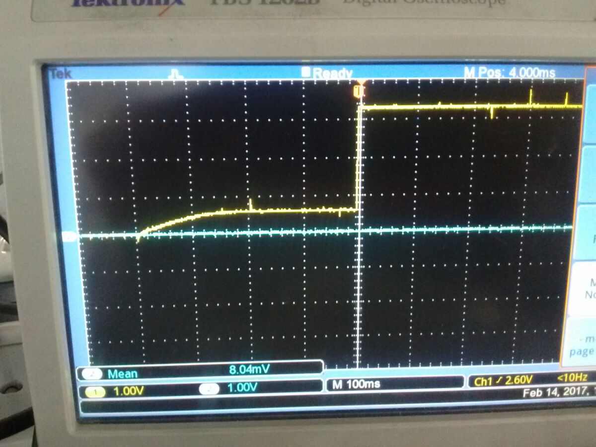
Please find the attached schematic, we are generating various rail (5V, 1.35V, 3.3V and 1.8V), we are doing power sequencing using PG output, When I am probing 3.3V rail, I am not getting the result as per web bench simulation. (Snaps are attached, it is taking almost 500ms to ramp up 3.3V )
Schematic is not the exact replica of webench. Kindly explain how extra components and their values will impact performance.
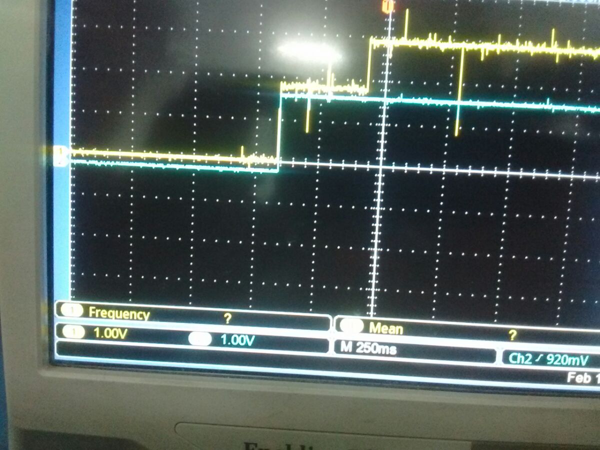
In one of the board we observed one behavior which we could not our 3.3 output voltage first becomes stable at 1.8 V for say 500 0r 600 ms then only it ramps up to 3.3V, (refer to fig 2)if i remove the load from this board by removing power to processor and image sensor it shows behaviour similar to fig 1
I have following question
1) Does value of pull up resistance on PG pin could cause T
2) How does adding extra Cap on EN pin and in shunt with feedback resistor impact performance.
Note: image 2 is showing 2.8 V as in image we probe after LDO which is generated from 3.3V, behaviour is same for input also.