This thread has been locked.

If you have a related question, please click the "Ask a related question" button in the top right corner. The newly created question will be automatically linked to this question.

WEBENCH® Tools/LM25085: Output voltage not regulated properly and weird behaviours

Part Number: LM25085
Other Parts Discussed in Thread: LM5085, LM2735

Tool/software: WEBENCH® Design Tools

Hello,

I have designed a DCDC regulator with the LM25085 controller with Webench and prototyped the circuit on a PCB. The circuit is designed to regulate the voltage to 16.5V at 1.2A, however the voltage output is not regulated properly. Output voltage turns around 2.16V. The device also has weird behaviors that will be discussed below.

Circuit design information

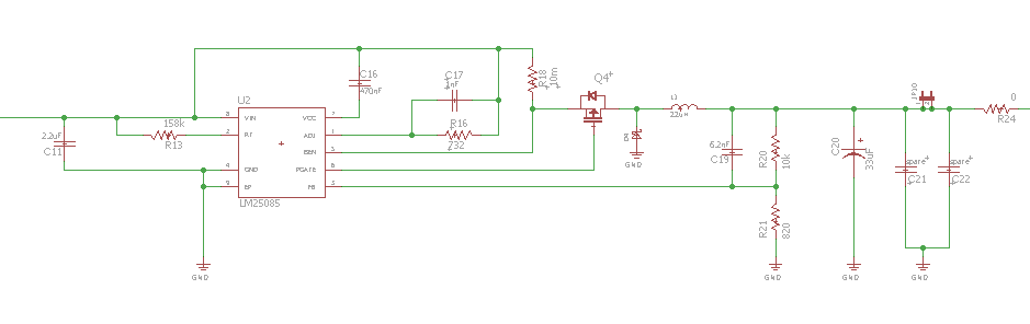
The circuit was designed to produce 16.5V at 1.2A for a 19 to 25V input voltage. The following image shows the design result.

The circuit has been mounted on a PCB using exactly the configuration of the above schematic. No load is plugged on its output. The output capacitor (Cout) is a tentalum capacitor, the exact one suggested by Webench.

Behavior #1 : Voltage is not regulated properly

First observation is when the input voltage (20V) is hot plugged to the circuit (power source already turned on when connecting), the output gets regulated to about 2.16V. The feedback pin voltage stays around 0.16V, way below 1.25V. I have noted the voltages at all pins of the device (probing with a multimeter in DC voltage mode). The following image shows the actual schematic with the probed voltages.

The weird one here is the FB pin voltage that stays around 0.167V rather than 1.25V as we would expect.

If we observe the switching scheme across the diode (D4), we can observe the following signal.

We can see a single pulse. This scheme is repeated about each 250 us with nothing in between.

Behavior #2 : Voltage regulated to 16.5V after shorted Vin and Vout

One interesting observation is that if we momentarily short Vin and Vout (which brings Vout to 20V momentarily), then the output voltage is regulated to 16.5V as it is supposed. It seems like it brings the controller into the correct steady state operation. However the output voltage drops back down as soon as a load is applied on its output (200 Ohms is enough to make it drop, 400 Ohms does not make it drop).

The switching scheme in this case is similar, but we can observe two larger pulses instead of one :

Behavior #3 : Ramping up the input voltage

If we ramp up the input voltage progressively from 0 to 20V, we observe a behavior that seems normal. We observe the following stages :

  • Vin = 0 to 3.9V : Vout = 0V (device in shutdown mode because of UVLO threshold)
  • Vin = 3.9V to 16.5V : Vout follows Vin
  • Vin > 16.5V : Vout stays at 16.5V

So ramping up seems to work fine at no load. If we ramp up with a 200 Ohms load, it seems to work fin as sell, however it drops down to around 0.5V or 0.6V.

Other information

  • The preceding behavior are observed on two distinct prototype with the same BOM and I have double checked the soldering to make sure there was no connection problem. Therefore it is unlikely to be a broken chip or connection problem.
  • I had another previous design working the the LM5085 (which is about the same as the LM25085). I tried to replace some parts to see if they could have an influence. I swapped the LM25085 with the LM5085. The Rt resistor was changed (to 100k, then 28.7k). The output capacitor was changed to an electrolytic 100 uF capacitor instead of the tantalum capacitor. The diode and transistor were also changed for other equivalents used in the previous design. None of the changes made the output regulate properly. The output voltage was not 2.16V anymore, but was not any interesting value, varying sometimes around 5V or 1.7V depending on the components.

Analysis and hypothese

Following those observations, it feels to me like the device does not go in a normal regulation mode somehow, like if there was something in the control logic that is limiting the switching of the transistor somehow. I've tried to figure out what could potentially be preventing the normal switching of the transistor looking at the functional diagram and the observed voltages.

The VCC UVLO should be fine since the regulated VCC is normal. I hardly think it could be a thermal shutdown issue. The package used has a power pad and no load is connected.The RT pin voltage is high enough for the IC not to be in shutdown mode. The voltage on ADJ and ISEN pin should not produce a overcurrent limit. Therefore I don't really see what could be going on further than that.

Conclusion

So, I've been analysing the issue pretty far up to now but still don't have an idea on where it comes from. Would it be possible, please, to get quick help in regard of this issue. Any idea on what could be going on here and/or how to fix this issue ?

Kind thanks in advance.

  • It is not unusual to have issues when hot plugging input power. It is possible that you can have over voltage transients or other abnormal conditions. Since the circuit works correctly wit a normal ramp up time, your schematic and BOM are most likely correct. You could try to capture start up waveforms, triggering on VIN rising edge to see exactly what condition is causing your hot plug issue (but of course hot plugging is not recommended).
    I am assigning this thread to another engineer who supports LM5085 directly. He may have additional comments.
  • Hello John.

    Thank you. Here are more details.

    - It does work when ramping up slowly, but not quite well when powering up our (Xantrex) power supply while connected. If the circuit is powered by powering up the power supply, the output stalls.
    - Even though we can get 16.5V on its output in a way, the system is unable to give the required power and the voltage drops back to about 2.16V (and remains there) when not much load is applied (as detailed on the first post).

  • Hello again John.
    Do you think it would be possible to get the contact infos of this other engineer?
    Thanks in advance.
  • I will forward this thread to him with high importance.
  • Hi John. I thank you.

    tl;dr
    Webench should recommend more input decoupling.

    I had a previously webench-designed another circuit using the LM25085 (and never used the board). The circuit was regulated currectly, but under load, the output voltage was (also) crashing. Increasing the input capacitance solved the issue apparently :-).

    DCDC_entree_LM25085_Vout_45.pdf

  • Hughes,

    Did increasing the input capacitance fix your issue? I did receive confirmation from the support engineer that he will look at your issue today. Please confirm your status.
  • Hello Hugues  (and thanks to John Tucker for directing me to this forum post.)

    If you hot plug manually by using a toggle switch or banana plug there is probably some contact bounce that may cause the Vcc input to get pushed below ground and cause a startup issue. Try adding the diode discussed in data sheet section "7.3.6 VCC Regulator" on page 14 of the data sheet. In general, any pin getting pulled below the substrate voltage can cause any number of oddball problems for an IC. I suspect that adding this diode would be wise in any application.

    If that does not fully resolve the issue then I would next look at the interconnect of the current sense resistor and routing to Isen and Iadj input pins. These two signals should be Kelvin connected to the end caps (pads) of Rsen so that trace inductances don't cause a sensing error.

    One other thing is that in some applications Webench give very low capacitance values for Cin. It chooses the capacitance based on the ripple current need for the application but bases this on a very optimistic view of the input power path. If you are in a bench environment with clip leads the Cin value given by Webench will be too low. Try paralleling the existence ceramic Cin with a low ESR Aluminum.

    Next - A word of caution about Tantalum caps as all or part of  Cin. Very few tantalum capacitor types are surge rated to survive hot plugging events. It is possible for a tantalum capacitor to failed very dynamically if used as Cin in a circuit that undergoes hot plugging.

    Let us know if we are on the right track to resolving your issue.

    Alan Martin

  • Dear Alan,

    I thank you for your answer. I successfully increase performance with more input capacitance. I respinned the board, I'll let this thread know if all problems are solved with proper decoupling.

    Best regards.

    Hugues

  • Dear Alan,
    I have a question for you: what are the common causes other than improper decoupling for a DCDC not being able to push its current rating until it reach its thermal shutdown?
    Regards.
  • We have many customer problems associated with incorrect PCB layout. This is a problem common to all power supply IC suppliers. There is a tradeoff in creating a data sheet that if you really want to convey information about the layout of a power path, that describing it in text is not really the best approach. The second best approach is to show "the factory layout" of an evaluation board of the IC. Often this is in a separate document for the EVM and it may not get provided to the person that does the actual PCB layout. A different issue is that the factory EVM may not represent the manner that the customer actually wants to use the device. There is a third factor. The schematic does not represent the true schematic the includes the device and PCB parasitic elements. The fourth factor is language barrier. When English is not the native language of the design engineer or the PCB layout person, then all the written layout guidelines tend to not be read and followed. We have some videos in the planning stage to try and resolve this communications problem with the designers of the end application. PCB layout is a 2D-3D interactive process. A simple text description of the PCB design is inadequate.

  • Dear Alan.

    I need your help again. ^^ I successfully increased the amount of output power of this DCDC when connected to a DC variable load. However, it simply doesn't provide any power when connected to a battery (which has a lower voltage than the regulated output of the DCDC), as a CC/CV battery charger. May I have a discussion with you over the phone, please? I will be pleased to share the solution with everyone in here afterwards. You need to know I experimented using the reduced ripple configuration, and increasing / decreasing various capacitances & inductances, unsuccessfully.

    Here's the schematic:

    Here's the layout:

  • Hello again Hugues,

    It's good you are having more success getting increased output power. But let's revisit the approach.

    You are asking for a CVCC power stage to charge a battery yet you are selecting a conventional buck regulator IC. Most conventional ICs of this sort do provide current limit, but this is a safety mechanism only to prevent device damage and overheating. This is not a smooth transition into a well behaved constant current operating mode. Just how the IC operates during current limit is unique to the design of the IC. Some ICs have hiccup mode, some trip off and stay off, some attempt to put out full current. I have seen ICs from other manufacturers where a 5A rated IC will put out in excess of 12A in shorted conditions - truly unsafe. Current limit behavior is sometimes discussed in the device data sheet and many times the description doesn't tell everything you might want to know.

    So in your application there are several factors. You are applying a constant-voltage control loop device into an application that really needs proper constant-current operation as well. So either find a CVCC device or apply additional active and passive devices to your selected IC to implement the CC operation mode.

    There is an  important point to be made. It is very wise to have an output blocking diode as you leave the charging power stage and enter the battery. Otherwise a circuit fault in the input source or power stage can be fed by the battery with "negative consequences". Keep in mind that without a blocking diode, the battery voltage can go backwards through the inductor and MOSFET and appear at the input. If the input is a user attached cable, say from a wall adapter, it a short occurs on the cable, then high currents can flow out through the input port.

    An additional point is that it you are going to use a CVCC power stage to fast charge a battery, you'd better have a way to sense when to stop the charge cycle. As a battery reaches full charge it starts dissipating the incoming energy as heat rather than storing the energy chemically for later reuse. Overcharging a battery will at the very least reduce its number of charge recharge cycles. Some battery types are very dangerous to overcharge.

    If you are not fast charging but using a CVCC stage and then float charging then the task is easier. Just make sure the battery manufacturer allows this charge and float mode.

    Attached are two different schematics for adding Constant current limiting to a CV-only power stage. (BTW - This approach WILL NOT WORK on conventional Boost stages, as they don't have current limit anyway.) The stages based on the dual transistors are small in size but look complicated in the schematic. It's all actually an easy add-on.LM43603_CVCC_4cell_NiMH_Charger_Sch.pdf

    LM2735_Sepic_CVCC_4cell_NiMH_Charger_Sch.pdf

    Hope these help. This stage can be applied to many Buck, Flyback or Sepic stages. It depends on the IC selected how well CC mode performs at zero volts output.

    Another thought; The voltage divider that set the CV mode voltage. This should really connect across the battery and past the output blocking diode. There really ought to be a disconnect fet so when input power is absent the divider resistors don't discharge the battery at all. This is shown on the LM2735 sepic approach.

    With all that said; there is probably a CVCC device from the battery charging section of TI - most parts start with BQ prefixes. You might look at the selection guides on the TI website or post a request in that forum.

  • Dear Alan,

    I thank you for the detailed answer. I particularly appreciate the comment on the voltage divider being wired after the blocking diode.

    I though the LM25085 was specifically designed for CCCV in mind. Here's a link to an application note in this regard. I though the additional circuit was only to provide an accurate current limit. Am I wrong?

    For your information, I agree with what you are saying in regard of overcharging & heat dissipation only in the case of batteries that include a redox shuttle mechanism. Simply put, what you are saying isn't always the case.

    Regards.

  • Hello,

    Thank you for referring me to that Ap note; I wasn't aware of it. My group just recently started supporting a large selection of the TPS prefix devices and we are still learning about the auxiliary uses.

    Yes, the discrete transistor circuitry is used to provide an accurate adjustable current limit to a regulator that does not have the required current limit behavior for a particular application.

    I agree that battery charging and all its subtleties is not my forte'. There are many chemistries to keep tabs on these days.

  • Dear Alan,

    No worries.

    Does the LM25085 support CC/CV charging, or it does only when combined with the circuit in blue in the Figure 2 below?

     My understanding is that the CC operation will be more precise with the blue circuit, but that it should work using Figure 23 of the datasheet.

    By the way, I found a bug on the E2E website ^^. Let say I want to insert an image: If I upload an image, decide to cancel, then, I edit the image locally, and want to upload the edited version of the image, unless I change the name of the second version, the first version of the image will be added to the post.