This thread has been locked.

If you have a related question, please click the "Ask a related question" button in the top right corner. The newly created question will be automatically linked to this question.

TPS56121: Output voltage abnormality at low temperature

Part Number: TPS56121


Hi,

I am checking the operation of TPS 56121 at low temperature.
I repeatedly turning on and off the input voltage and measured whether the device operates normally.
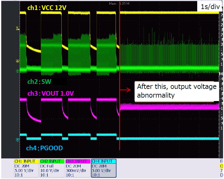
Attach a waveform. The output voltage does not operate normally when repeating on and off several times.
The condition that does not operate normally occurs when the temperature is lowered from -35 ° C.
Are there any possible causes?

Best Regards,

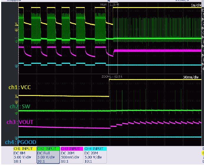
  • I have not seen that specifically before for TPS56121. Are you using the TI EVM, or your own circuit? Usually these types of cold temp start up issues are caused by poor layout, typically with respect to input capacitor placement. How are you cycling the power quickly? Can I see the waveform zoomed in on the red line area?
  • Thank you for your reply.
    This board is my own board, not EVM.
    Attach a waveform with an enlarged red line.
    The duration of the on / off cycle is not particularly determined. It is on / off manually.
    However, if the off period is short, abnormality of output voltage is likely to occur.
    In addition, this phenomenon does not occur when the input voltage rises from 0 V.

    Best Regards,

  • Can I see your schematic and layout? Also I will need more waveforms. The exact voltage levels will be critical. Therefore you need to ensure that all the ground references are exactly on major axis grid lines. Also they need to be the highest resolution images you can manage so I can examine the fine detail. I don't need to see PGOOD, instead substitute EN/SS for one picture and ILIM for the next. Please zoom in a little further as well. Thanks.
  • Hi,

    I measured the operation of EN/SS pin and ILIM pin.
    Attach the measurement waveform. The attached waveform is an enlarged waveform of abnormal and normal waveforms.
    Are there other pin waveforms that I need to see?

    Best Regards,

  • Your EN/SS pin is resetting. That is why the voltage is not regulating correctly. Now the trick is to find out what is resetting it.
  • This is probably one of two issues:
    1. Possibly OCP hiccup mode. Please zoom in on the first rest of the EN/SS and count the number of switching cycles. If it is about 4 then it is OCP.
    2. It may be possible that you have a race condition with VIN UVLO and EN/SS enable voltage threshold. EN/SS needs to be pulled below 270 mV to ensure the device is reset. Or the input voltage needs to be pulled below the UVLO. Can you vary the timing between on and off to ensure these conditions are met?

    Check these two things please.
  • I'll definitely need to see that zoom in of the first series of switching pulses. Please make sure the timescale is such that I can measure the on time and frequency.
  • The unusual thing about this part and their configuration is that switching frequency is programmed by detecting the ground resistance on the COMP pin, and it’s possible that on restart, the part is detecting the wrong ground resistance due to the residual voltage on the COMP pin. If the part is recovering to 300kHz instead of 1MHz, the inductor ripple and loop compensation may be inappropriate, resulting in and over-current.

    I would check the SW pulse frequency with a 10us/ division “zoom” of the faulty restart attempts to see if they are coming up at 300kHz on the faulty restart.
  • Thank you for your reply.
    And I'm sorry for the late contact.
    I will inform the result of the measurement.

    The upper waveform of the attached is the waveform when EN/SS is reset. CH3 is the measured waveform of the inductor current.
    The switching frequency is 500kHz. Sorry, I did not say that R406(13kΩ) is not implemented.
    Therefore, the switching frequency has not changed.
    The inductor current shows that it reaches near the overcurrent detection level.
    The ILIM resistance is 1kΩ, so the overcurrent detection level is 10A. So it's almost as set.

    Therefore, I think to increase the ILIM resistance and enlarge the EN/SS capacitor in order to lower the inductor current at startup.
    However, I think the overcurrent detection level varies with temperature.
    The figure below is measured in an environment of 25℃, but overcurrent detection does not operate even when the peak current of the inductor is 14A. Valley current is 12A.

    I want to ask you a question.
    (1) Overcurrent detection level is determined by ILIM current source (25 ℃, 10uA).
      Is it possible to show data to me how much its value fluctuates between -40℃ and 125℃ ?
    (2) Can the valley current detected by the low side FET be considered as the lowest value of the inductor current?
      I think that the lowest value is the valley current, not the average value of the inductor current.

    Best Regards,

  • The ILIM current can vary a lot from about 7.5 uA at -40 C to about 14 uA at +125 C.

    Valley current is the current lowest level during the low side on time.

  • Thank you for your reply.
    I am very thankful for your response so far.