This thread has been locked.

If you have a related question, please click the "Ask a related question" button in the top right corner. The newly created question will be automatically linked to this question.

TPS5410: ESP8266 keeps rebooting with TPS5410 - I see a clear difference in the PH signal - need explanation

Part Number: TPS5410

I have a design that integrates a TPS5410 based DC/DC converter to provide 3.3V to an ESP8266.

After building up a small bach of prototypes, I have some where the ESP keeps rebooting periodically which is generally associated with an issue on the power supply.

I have a 100nF ceramic capacitor right between 3V3 and GND at the ESPs VCC pin and a 470uF electrolytic capacitor to ground directly at the 3V3 output at the DC/DC stage (right behind the inductance)

Looking at the scope, I see around 50-150mV high frequency content on the 3V3 line at the ESP, but there is no significant difference between the good and the bad parts. I have tried triggering off the serial output to see when the reset happens (usually, the part needs about 30ms between the reset and the first boot loader messages) but was unable to find anything unusual on the 3V3 line happening up to 1.5s before the reboot.

I then turned to the DC/DC stage itself and found a marked difference in the PH signal:

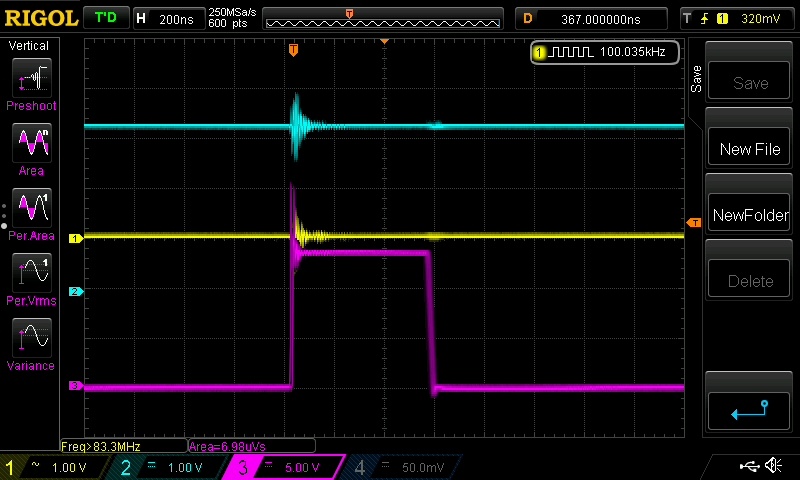
this is a good part, apart form some ringing, the rising edge looks like it does in the datasheet

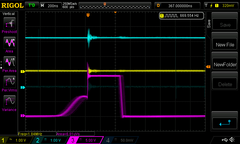
This is one of the bad parts, notice the shoulder before the rising edge of the PH signal. This shoulder is present with all the troublesome parts I have looked at and absent with all the good parts.

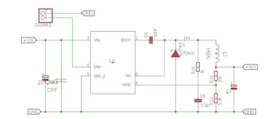
this is the dc/dc stage, please note that the output capacities are drawn on the digital part of the design sheet, but are in fact across 3V3 and GND with the values given above.

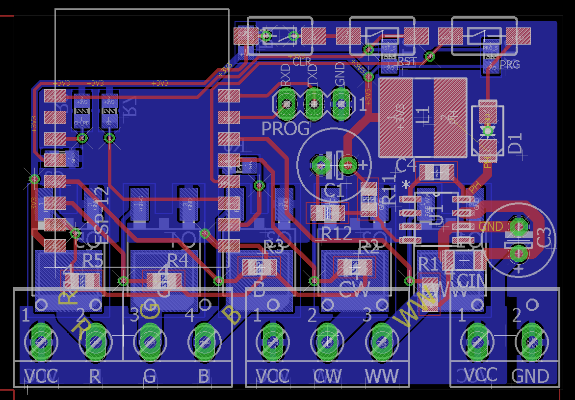
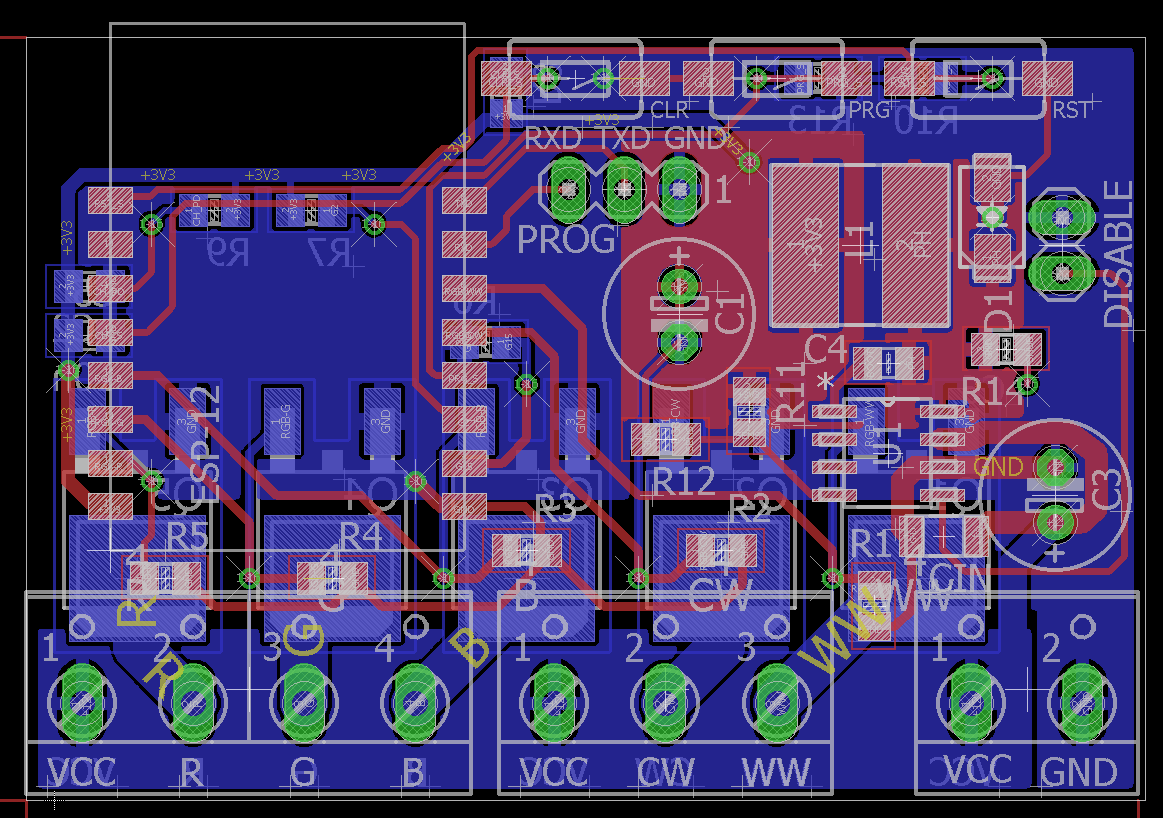
here's the board layout. My ground reference for the traces above is the gnd pin on the ESP (the bottom layer is 2/3rd GND flood filled, so the highest GND impedance would pe the short trace from the pin to the VIA and the VIA itself - neglectible in my view.

C1 is directly across 3V3/GND at L1
C2 is on the bottom layer across 3V3/GND a few minimeters from the 3V3 pin

C3 and Cin are very close to the TPS5410

I assume there is something wrong in the direct vincinity of the TPS5410, creating that strange shoulder - I have measured C4, D1 and L1 for correct solder points as I have all the pins of U1(the TPS5410)

It should be noted that at the time of taking those traces, there was no current through the MOSFETs on the bottom side nor were they being switched.

I would appreciate any help in figuring out what creates this switching behaviour and if it could be the source of the issue I'm seeing - it certainly correlates with it.

the eagle files are here: github.com/.../v2.2

kind regards

pj

  • Peter,

    It looks like the difference between the two switching waveforms is due to the load current.  The top waveform is CCM and the bottom waveform looks like DCM.  If you increase the load current, does the bottom waveform circuit switching waveform start to look like the top one?  Your issue with noise is most likely due to the layout.  I can'y look at your eagle files right now, and the layers in your "pictures" folder don't seem to match what you have posted. It appears you have just a two side PCB with the VIN, 3.3V, GND and SW nets all connected by regular thin copper etch lines.  Typically you will need a ground plane or large copper pour area for GND.  The circulating current loops need to be a tight as possible connected with copper pour areas.  Especially important is your return connection for D1 and tightly coupling your input capacitors directly to VIN and GND pins on the IC.  See the datasheet layout guidelines on page 22:

    And the EVM design here for examples:

    www.ti.com/.../slvu185.pdf

  • Hi John,

    thanks for your quick feedback. Most of the bottom side of the layout is taken up by a GND flood fill area, I had just not shown it in the screenshot. With flood fill shown, the layout loosk like this:

    But if I understand you correctly, the sinusoidal "shoulder" in the trace shown above indicates higher load?

    I had turned measuring the area under the pink trace on - as you can see, the (wider) upper signal (of the good part) has a slightly higher area of 6,98µVs vs. 6,81µVs in the lower case, also, I would have assumed that the steeper edge of the 1st signal would induce a stronger magnetic field in L1.

    I will double check the solder joints on D1 (which has a large, direct GND connection through a VIA underneath it, but I can probably stich some more for a lower resistance path (the single trace from D1 to the PRG switch is just a GND tap for that Switch, not GND for the diode).

    I would assume that the worst bit of the design is the fact that the 3V3 line has to snake around the GND layer to the other side of the ESP chip, but then again, that chip should not take more than about 200mA peak, but I certainly can add a bit more capacity on that side.

    kind regards

    pj

  • Peter,

    Actually, it is the other way around. Since TPS5410 is non-synchronous converter, when the load current falls below 1/2 the p-p ac inductor current (85 mA/2=42.5 mA), the device enters DCM (Discontinuous Conduction Mode). If there is no changing current in the inductor, there can be no voltage across it and Vsw = Vout. When the current initially goes discontinuous, the SW (PH) node will ring and eventually settle out at Vout. In your case, the next switching cycle begins before the first half cycle of ringing completes. So if the load current is above about 43 mA, you should see waveform 1 and below 43 mA, you should see waveform 2. In any case if you suspect the switching noise is causing your ESP to reset, you can:

    Increase the capacitor filtering. I would use a low value ceramic capacitor whose resonant frequency is as close to the switch node ringing frequency as possible (probably around 0.01 uF or o.001 uF)

    Clean up your layout to reduce further the ac circulating current paths.

    Ad an RC snubber from the PH to GND.

    Hopefully one of the above will help.
  • Hi John,

    thanks for the exhaustive response. I'll make a few updates and see what happens.

    kind regards

    pj
  • So I've updated my design in three ways:

    a) I've added flood fill areas for PH and the 3.3V Node

    b) I've added a snubber with 1kOhm / 1.5pF to the PH node to ground

    c) I've added a 10nF capacitor as close as possible to the ESP 3.3V input.

    are those flood fills for 3V3 and PH generally a good idea as low impedance paths?

    I shall have boards made and test them.

    pj