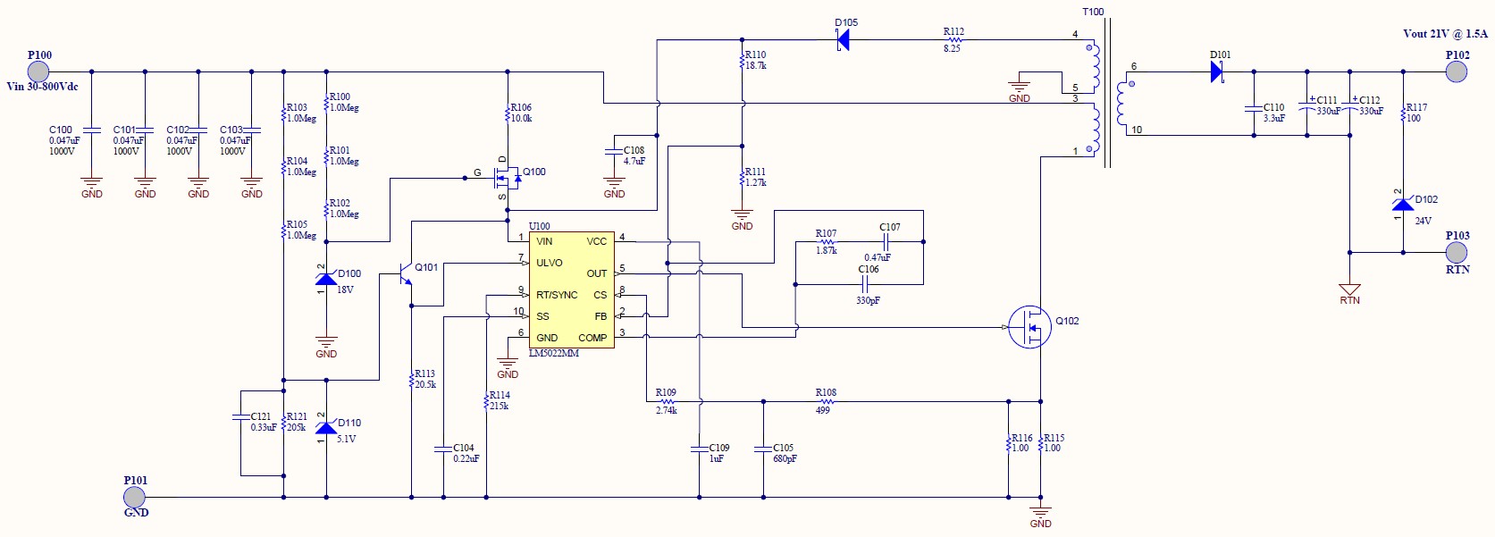
HI TI experts,
could you be so kind and tell me what if the function of the R116 resistor in the PMP7764 TI reference design:
This thread has been locked.
If you have a related question, please click the "Ask a related question" button in the top right corner. The newly created question will be automatically linked to this question.
HI TI experts,
could you be so kind and tell me what if the function of the R116 resistor in the PMP7764 TI reference design:
Hi Youhao,
Thank you for your replay but, is it just your understanding of the application or it is really so?
Could you explain a bit more how can I calculate the needed resistor value?
How can I calculate the resistor value? Is there any defined dependency I should consider between input voltage and switching current?
There is other reference design from TI - NSC1024 (old National Semiconductor nomenclature) - very similar one but without this resistor???
could you tell me why one reference design have this feature and the other one haven't?
Thank you for your support!
and have a nice weekend :)
Best regards,
Tomasz
Answers to your earlier post regarding the transformer: The inductances of the winding of (1-3) is 3mH +/- 12%. Leakage 50uH.
Regarding your question of R116, its purpose can be seen in the following analysis. Assume Lm is the inductance, Fsw the switching frequency, k the transformer turns ratio, and the load current Io. Then, the duty cycle at a given Vin is:
D = Vo /(Vo+Vin/k)
The transformer peak current in the primary winding is:
Ipk = Io / [k x (1-D)] + Vin x D / (2 x Fsw x Lm)
Therefore, the peak current limit (IPK) is tripped, the load current is
Iomax = [ IPK - Vin x D / (2 x Fsw x Lm) ] x k x (1-D)
The load power when peak current limit is tripped:
Pomax = Vo x Iomax
Substitute Io and D into above equation, you can find that Pomax will increase with Vin. To prevent Pomax from being excessive, you should reduce IPK when Vin increases. The simple way to do this is to use R116.
As I mentioned earlier, R116 introduces an DC bias voltage to adjust the peak current limit: Vin x (R108+R109) /(R108+R109+R116) to VCC, superimposed to the CS current signal Ipk x R115. Higher Vin will add more dc bias, effectively reducing the actual peak current IPK allowed through R115.
Roughly, the effective peak limit will become (converting to sense voltage):
IPK x R115 = 0.5V - Vin x (R108+R109) /(R108+R109+R116) - 45uA x (2k + R108 + R109) x D.
Where 45uA is the internal slope compensation current, and the 2k resistor is also internal.
You can see, having R116 prevents the overload from being excessive when Vin increases. Working out the math you can find out the proper R116 needed.
Hope this clarifies.