This thread has been locked.

If you have a related question, please click the "Ask a related question" button in the top right corner. The newly created question will be automatically linked to this question.

TPS61030: Issues with TPS61030

Part Number: TPS61030
Other Parts Discussed in Thread: TPS61230, TPS61230A

Hello everybody,

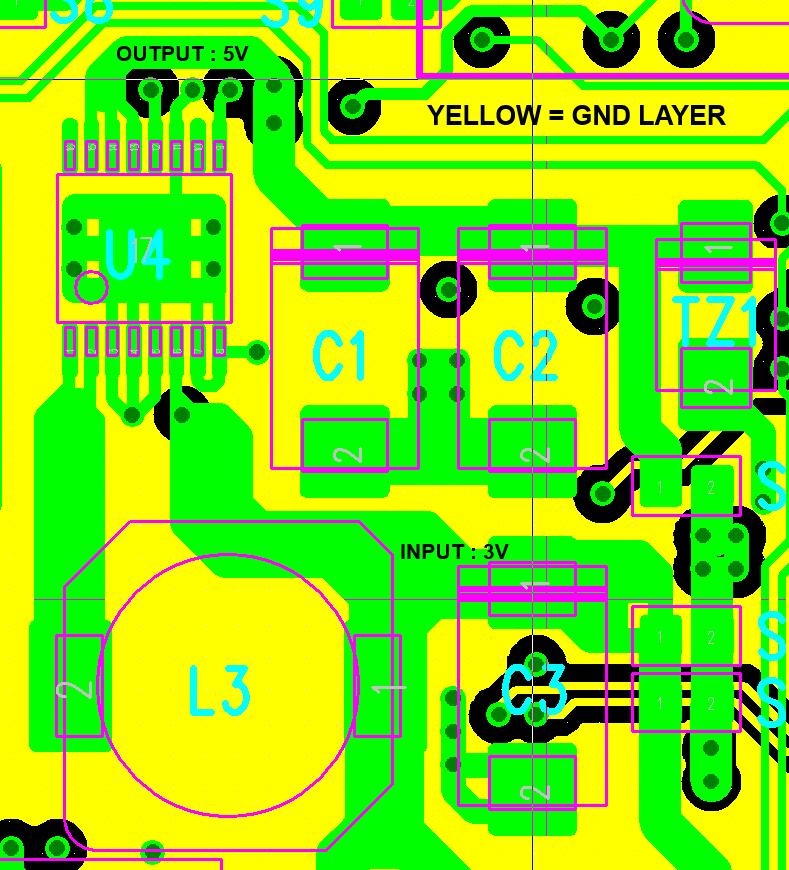
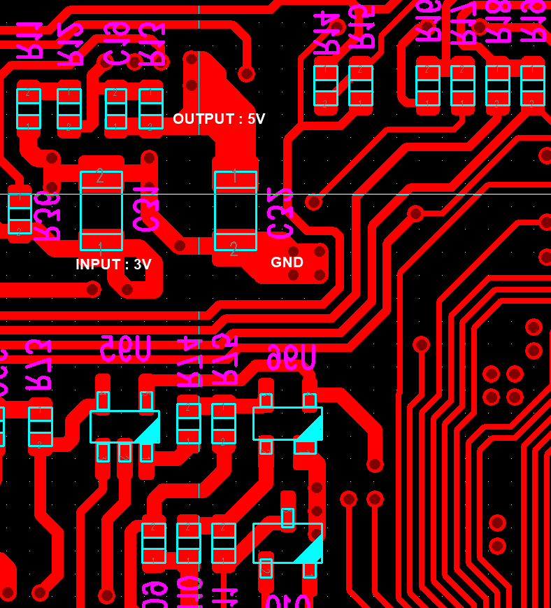
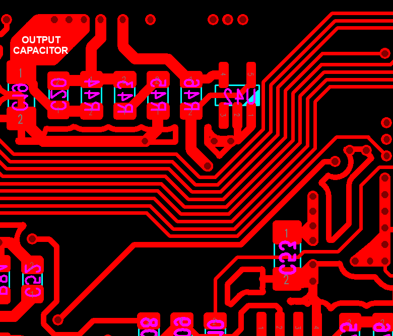
We are using a TPS61030, as a power supply for our product (a calculator for off road vehicles). You can see our schematics attached to this post.

We are experiencing some issues with this product. We already have two problematic cases. In those two cases the TPS61030 is returned broken from our client (approximately after 1 year of service). The component is in short circuit state.

We already have check our calculation for passive component selection (inductor, capacitor, feedback resistor) and the power rating of the TPS61030 compared to our need. For your information we have done the calculation for 1A output current (5V) and the measured current consumption is less than 250mA.

So we would like to have some help to find the root of this problem.

RegardsPower supply UC402.pdf

  • 1. does the SW short to GND in the fail device?
    2. could you share you layout?
    3. what is the fail rate
  • Hello Jasper,

    Thank you for your answer.

    You will find attach to the post the layout of the power supply (Green = Top Layer, Yellow = GND Layer and Red = Bottom Layer).

    The fail rate is 3 for 500 pieces. The fact is that we don’t have delivered all these pieces at once. And most of them were delivered recently. So we don’t really know yet the ampler of the problem.

    On the device that we measured the SW is effectively shorted with GND pin.

    Here is the schematic :

    And the layout :

    Regards

  • The layout is not good. the routing between the IC and output ceramic capacitor C32 is a little long. This could cause high voltage spike at SW pin that has risk to damage the IC.
    as the process variation, some IC are damaged, most of the IC not. and the damage could happen after long time operation.
    this application is about how to optimize the layout www.ti.com/.../slva773.pdf
  • Hello Jasper,

    Thank you for your answer.

    We have a few more questions:

    We are using the same component in other products. On those products we didn’t have any issue yet. I attached to this post the layout of the three other products that are using TPS61030 (the color coding for the layer is green = top, red = bottom and yellow = internal layer). Could you tell us if we risk having the same problem on them?

    UPC 401: U3 = TPS61030 and C40 = Output capacitor

    UPC403: U8 = TPS61030 and C37 = Output capacitor

    UC234: U1 = TPS61030 and C19 = Output Capacitor

    And then could you give us a method to measure on our product if the spikes on the SW pin will potentially damage the ic.

    Finally could you give us a maximum distance that is acceptable between the ic and the output capacitor. Because we thought that the ic is very (too much?) sensitive. A few millimeters more seems to be sufficient to destroy the power supply.

    Regards

  • One more question : Do you have an equivalent component (with the same package) with better caracteristics in term of voltage spikes robustness ?
  • The layout are not optimum, but better than the first one. the ceramic capacitor should be as the same layout of the IC, the routing between the IC and the capacitor is short and width. following is the method to measuring the voltage spike
    www.ti.com/.../slea025a.pdf

    not sure about the input voltage. but you can have a look at TPS61230 and TPS61230A. but the output capacitor is also needed to closed to the IC.
  • Hello Jasper,

    Thank you for your answer.

    We have done the measurement following the application note that you suggested to us. With the shortest possible ground wire we managed to reduce the the voltage spike that we measured.

    However we don’t manage to measure any differences between our different layouts. We are quite sure that the probe is magnifying the spike phenomena.

    So the main issue for us is to be able to confirm if our layout can be considered suitable. How could we be sure that the component will not fail again in the future? Could you tell us if in your opinion the layout that we submitted to you are suitable?

    Regards

  • are you setting the probe bandwidth to the maximum value? 500MHz or higher? what is the voltage spike in SW pin?

    what i want to see about the layout is that a 2.2uF ceramic capacitor is in the same layer with the IC, placing closed to the IC and routing directly with wide copper.