This thread has been locked.

If you have a related question, please click the "Ask a related question" button in the top right corner. The newly created question will be automatically linked to this question.

TL5001A: Short circuit protection

Part Number: TL5001A
Other Parts Discussed in Thread: TL5001

Good afternoon.

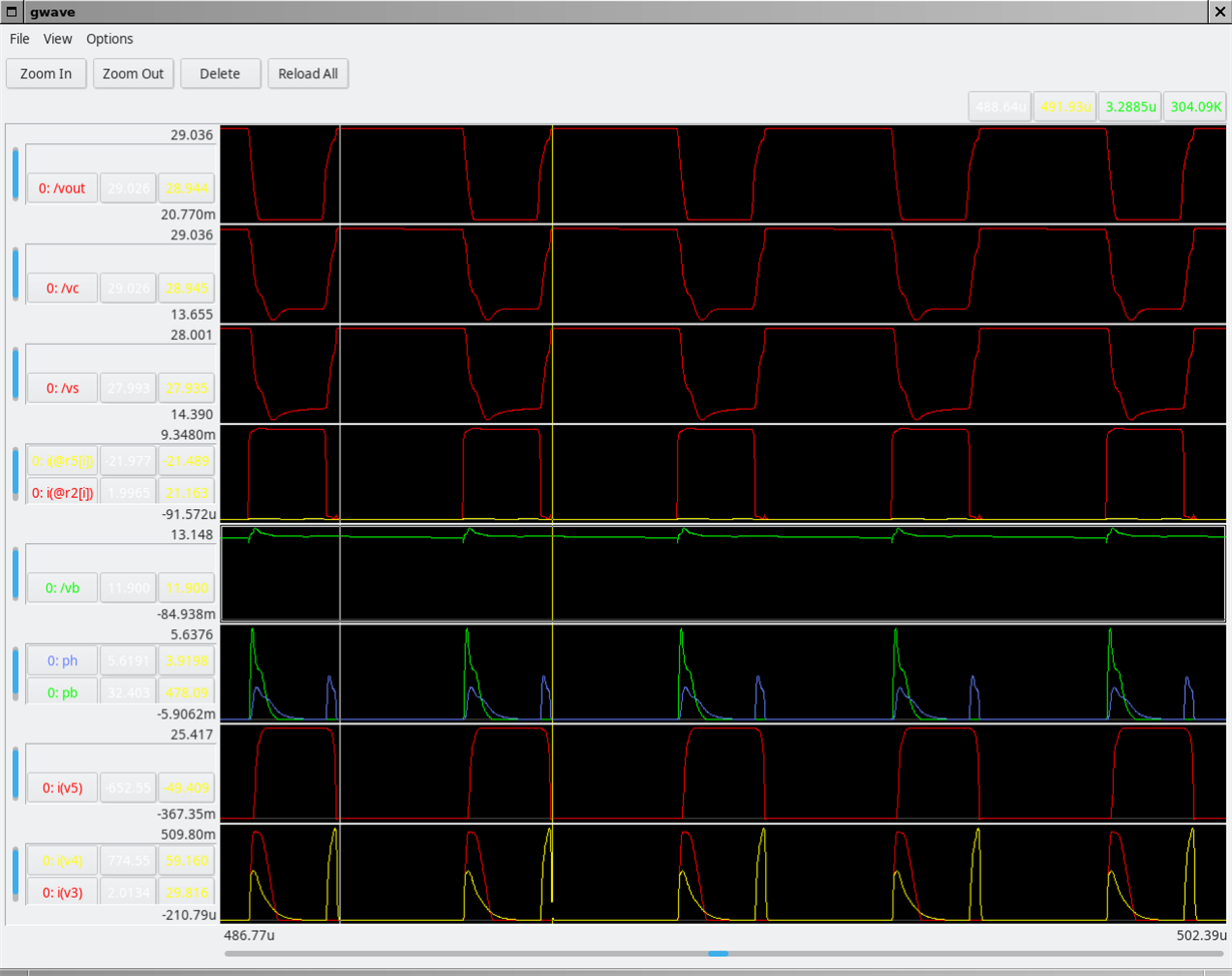
A few days ago, I was asking a question about a noisy self. I have done some tests and computed a snubber. Now, my schematic is :

I have added feedback divider by hand. I only use a simple divider with a capacitor.

Output power should be 200W (20A).

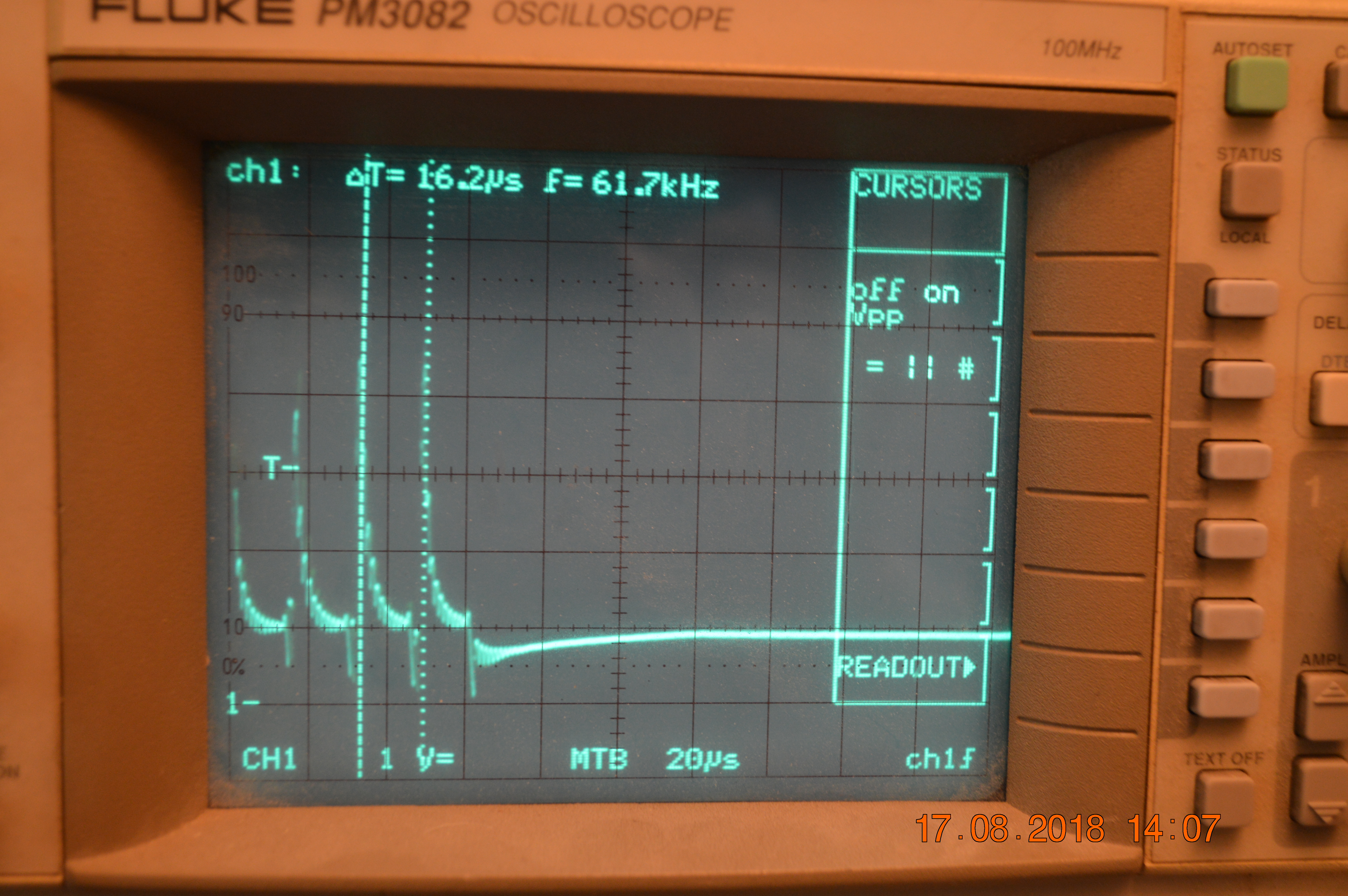
Whatever the output current, SCP signal remains greater than 1V. First diagram corresponds to a 100 mA output current :

First signal is output (11,5V). Second one is SCP signal. I have tried to modify C32 until 10µF without any result. Global efficiency is only about 65 % (!) when load consumes 6A.

Second diagram corresponds to a 6A output current :

Same constatations. SCP signal is too high.

I suppose I have done a mistake. In a first time, I don't understand why SCP signal is always greater than 1V.

Help will be welcome.

Best regards,

JB

  • I have found an issue in feedback circuit.

    Now, feedback circuit is :

    OUTPUT --- (10kR//(1.5kR + 22nF)) --- FB --- (100pF//(15kR + 18 nF)) --- COMP

    But there remains another problem. This circuit was designed to run with a 28V power supply and has to works at 300 kHz and it only runs at 75 kHz (I have tried to decrease Rt until 820R without any result, maybe Rdtc has to be modified also but I don't find any information in datasheet).

    Regards,

    JB

  • Hi JB


    May I know why do you select this device? it is hard to design and I expect the efficiency is very low, especially use NPN switcher and 300KHz frequency. I believe there are lots of IC with better performance.

    If you insist on using this device, please give me some time to understand this IC. Note that it is released at 1994. I should be able to reply you next week.
  • Hi Jasper. I use this device for several reasons :

    - DIP package;

    - Vin greater than 28V ;

    - usable for Buck, Boost, Flyback and inverting topologies.

    I have fixed half of issues, datasheet doesn't explain how compute feedback and compensation networks. Now, my TL5001A starts but doesn't run at 300 kHz, only at 75 kHz. I don't use this controller with a bipolar transistor but with a MOSFET and its driver.

  • Some news...

    First,my current schematic :

    SCP doesn't not exceed 0,2V. DTC is around 1,5V.

    First constatation : R28 (Rt in datasheet) fixes controller frequency. I have done some tests with 27k, 39k and some other values, I think that frequency is always around 65 kHz. I don't understand why I'm unable to fix this frequency at 300 kHz.

    Second constatation :

    This signal is taken on pin 7 of TL5001A (RT) for a 28Vdc power supply and a load that consumes 100 mA. If load consumes 1A, result is very similar.

    I don't know how analyze this measure. I suppose delay between two pics is the frequency clock. But, why does this clock stall for a long time around 1V ? Controller runs as expected during a few cycles and seems to stop for a few moment before restarting. I'm not sure this behavior is normal. For me, if load consumes enough current, controller has to switch every cycle.

    Best regards,

    JB

  • Hello Jasper,
    I think I have found half of the solution. I have to quicker discharge Miller capacity of the IRF9540. With a stronger polarization of the PF5102 (10mA), controller works better (@ 200 kHz, without bursts) but Q8 sees 14V/650mA when this capacity is discharged and ends up burning.
    Regards,
    JB
  • Hi JB

    Where do the 650mA come from? The circuit should limit the current through Q8. or we can add a resistor to limit the current.
  • Hi Jasper,

    The 650 mA comes from both grid capacity of Q10 and bootstrap capacity C37. Q8 can drive 650 mA but Q8 emitter voltage is between 14V and 28V (in my case as Vcc=28V). Thus, Q8 dissipates too much power and burns causing the death of Q9 (for the same reason). I have added between Q8 collector and ground a 1N5349B (zener with Vz=12V) and now, both BC327 and BC337 dissipates around 270 mW and the Zener only 510 mW. I can limit the current in Q8 by limiting its base current. It's easy, I have only to increase the value of R30. If I do that, Q8 collector current is weaker, but this current is not enough to discharge Q10 grid capacity when controller runs at 300 kHz.

    I haven't tested with a real circuit, I have to make a new PCB to do that.

    Best regards,

    JB

  • And results of Spice simulation :

    i(v3) and i(v4) are currents in BC327 and BC337. Vs is MOSFET grid voltage. Ph and Pb are power dissipated by BC327 and BC337.

    Regards,

    JB

  • Hi JB

    What is the definition of the grid voltage of the MOSFET? is it the connection point of the Q4, D9 and inductor? from the circuit, it seem the mosfet Q4 can't discharge to zero by the Q3

    I strongly suggest to find a real buck controller/converter. we can select package that is easy to solder. The circuit is too hard to debug, which also mean reliability issue.
  • Hi Jasper.

    Please note that Q4 is a channel-P MOSFET, not a channel-N one. Thus Vgs is the voltage between source (pin 3 of Q4) and grid and grid capacity should be discharged through Q2.

    /Vs is the grid voltage. You can see that it varies between 28V (power supply) and around 14V. Thus Vgs varies from 0V to -14V.

    Best regards,

    JB
  • Hi JB

    then it make sense. but I still think why you add the diodes in the driver circuit. could we use a circuit as shown following? is there issue with this circuit.

  • If you remove the Zener diode connected between collector of PNP BJT and ground, you will destroy this transistor. Diodes have been added to bootstrap Q2 by C6 (there are also Miller's capacities in both PNP and NPN). You can use your design (with of course the missing Zener), but you won't have a good efficiency if you want to run at 300 kHz.
    Regards,
    JB
  • Another problem in your design. You have to saturate the MOSFET. If you keep a Zener in 5001's out circuit, you cannot assure that Vgs will be greater than Vth. And you cannot assure also that Vgs will always lesser than Vgsmax.
  • Hi JB

    I see similar circuit in the datasheet page 2, but without the PNP/NPN. I guess you are right, the switching frequency can't be up to 300KHz.
    thanks for you comments.
  • Hi JB

    I closed the thread as you had resolved the issue. Just reply the post if further questions about the IC.
  • Hi Jasper,

    Some news. I have received my new PCB and I have done some tests with a load that consumes 8A.

    TL5001 now runs as expected (@ 300 kHz). @300 kHz, efficiency is not very good (between 60 and 65%). @100 kHz, I have measured 80%. If I reduce frequency, I can reach 90% but, in my case, I have to use a higher switching frequency.

    Another little trouble. If Vcc is not null when power is switched on (for example if circuit contains a filter before TL5001), sometimes TL5001 doesn't start as this circuit seems to require a very quick power on. I have added a depletion mosfet that completely discharges filter capacities between power supply and TL5001 to fix this issue.