This thread has been locked.

If you have a related question, please click the "Ask a related question" button in the top right corner. The newly created question will be automatically linked to this question.

CSD95379Q3M: suitability for two-quadrant operation?

Part Number: CSD95379Q3M

Hi,

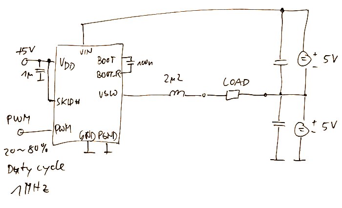
we want to use this part to drive an inductor that is tied to VCC/2 on its other end. Current needs to flow in both directions. This part seems to be suitable for this when used in forced CCM. As there is no evaluation board available for this product (is there a similar type that does have that?), I am asking if the part can be used this way, or if there might be caveat's to consider.

Cheers

Frank

  • Hi Frank,

    We will get back to you on Monday.

    Regards,
    Weidong
  • Hi Frank,

    Could you please send us the schematic or a circuit drawing? Do you want to use it as a buck-boost? what is the duty cycle? when you mentioned VCC/2, do you mean VIN or VDD?

    Please provide more information before we can answer your question. 

    In addition, we do have CSD95379 single-phase EVM available for buck converter.

    Thanks!

  • Hi,

    here is the circuit sketch that I have in mind. There will be hundreds of this building block, and the main PSU is in the kilowatts region. The load current must be controlled and be bidirectional of up to +/-10A. The load is a resistor of a few hundred Milliohms. The idea is that 50% PWM duty cycle will result in approximately zero load current, >50% will be positive load current, <50% will be negative load current. My only concern is if the driver chip can be used in this way because as a buck converter, it was designed with positive output current in mind, and not negative.

    Can you give me a reference to the EVM board that you mention? I cannot find that, neither Digikey, Mouser, Farnell.

    Cheers

    Frank

  • Hi Frank,

    The driver should work for your configuration with proper timing: PWM Low should always go first before PWM high at power-on, the reason is below: the output is at high voltage before power-on, it will require PWM low to turn on LS FET and pull Vsw low to have the Bootstrap cap charged before HS FET can be turned on normally.

    However, I noticed that your design has 7MHz operation frequency and 20%~80% duty cycle which CSD95379 cannot support. The driver IC has minimum HS off time (>100ns) and minimum HS on time which limit the operation frequency and duty cycle. As datasheet specifies, the max operation frequency is 2MHz.

    We don't have web-orderable EVMs available for this part. If you need one, please contact local TI sale team to help.

    Thanks!

  • Hi,

    we cannot guarantee to start with PWM low, as the driver will be enabled and disabled frequently and asynchronously. As the datasheet does not explicity state that the bootstrapped HS driver would have a separate UVLO, so your concern is partial MOSFET turn on and excessive heat generation, correct? If that is the case, we can test for this condition. I am not worried too much, as the maximum duration is one microsecond, and the inudctor is not carrying current yet (we can ensure this).

    Operation is a 1MHz, this is the European style to write the digit '1' :-)

    Evaluation circuit is already arranged, anyway thanks for offering.

    Cheers

    Frank

  • Hi Frank,

    When you mentioned the driver will be enabled and disabled frequently, do you mean to shut down the driver by pulling VDD low or just shut down the FETs with PWM tri-state? 

    The driver does require certain BOOT voltage for proper operation when PWM is activated and changes from Tri-state to High then to Low, there is possibility that the gate driver might not work properly when BOOT voltage is below certain value and not turn on the FETs. Enabling driver with a PWM low will eliminate this possibility.

    Thanks!

  • Hi,

    thanks again for your quick response!

    We'll generate a global PWM, and enable/disable individual channels by asynchronously tristating their PWM signal with a 74HC126. Making things worse, the PWM can also be inverted channel wise. That's why we cannot control the initial PWM state that the driver sees.

    I fully understand your concern, I've been desiging bootstrapped power stages up to 25kW in the past. My only question is, could starting PWM with HIGH for up to 1 microsecond damage the driver, assuming that inductor current is zero at that time? If it is just a glitch because the high side MOSFET doesn't work properly for this short period, then that's not a problem for us - as long as the circuit recovers from that in the next cycle.

    Cheers

    Frank

  • Hi Frank,

    Enabling driver with PWM Tristate to high while Vsw voltage is high will not cause driver or MOSFET damage as long as the peak current is within MOSFET spec. The risk is there is possibility that the driver might not respond to PWM or respond to PWM after uncertain PWM cycles when PWM exits tristate if starting with a low BOOT voltage and PWM high. This is because some circuits in the driver IC is not functional when BOOT voltage is lower than certain value. Sure this might not happen depending on the operation condition of the circuit, but we always recommend to start with PWM tri-to-low to eliminate the possibility of this risk for this type of applications. 

    Thanks and have a good weekend!

  • Hi Bo,

    thanks! I'll assess that carefully when testing the design. One last thought: as the load is very low impedance (basically a resistor), and it is tied directly to VIN/2, this means that the VSW voltage is also VIN/2 whenever the chip is tri-stated. Would that cause the bootstrap capacitor to remain partly charged, so that we won't have this problem at all? Or would an external diode between VIN and BOOT be a solution?

    Cheers

    Frank

  • Hi Frank,

    I don't think that adding an external VIN to BOOT diode will make any difference.

    If the output voltage can be maintained at VIN/2 or lower during PWM tri-state, the bootstrap cap will be partially charged and could work fine. 

    Thanks!

  • Hi Bo,

    thanks, that definitely eases my worries. I wasn't sure what the "diode emulation" bootstrap charging MOSFET would be doing when the device is tristated, but this means that that switch is closed, correct?

    Cheers

    Frank