This thread has been locked.

If you have a related question, please click the "Ask a related question" button in the top right corner. The newly created question will be automatically linked to this question.

TPS74401RGWT

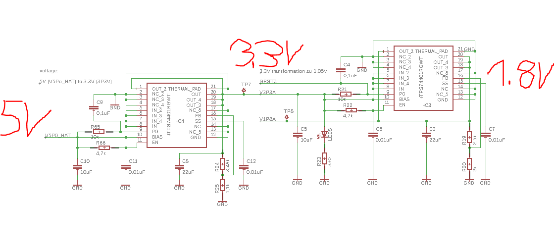
 on the Picture you could see my voltage design. is this design correct?

  • Hi Mario,

    The schematic you provided will generate the 3.3V from 1st stage and 1.8V from the 2nd stage. Please see my additional comments as followings:
    1. You have PG connected to the Vin. Usually PG is tied to Vout because when device is disabled, PG path won' t sink current due to Vout is OFF. When you have PG connected through a resistor to Vin, you will have a constant path to ground even you have the device disabled.
    2. You don't have to put the resistor between Vout and Enable pin.

    Regards,
    Jason Song