This thread has been locked.

If you have a related question, please click the "Ask a related question" button in the top right corner. The newly created question will be automatically linked to this question.

Problem with LM5576 - Dies on short circuit! - PCB Layout Issue

Other Parts Discussed in Thread: LM5576

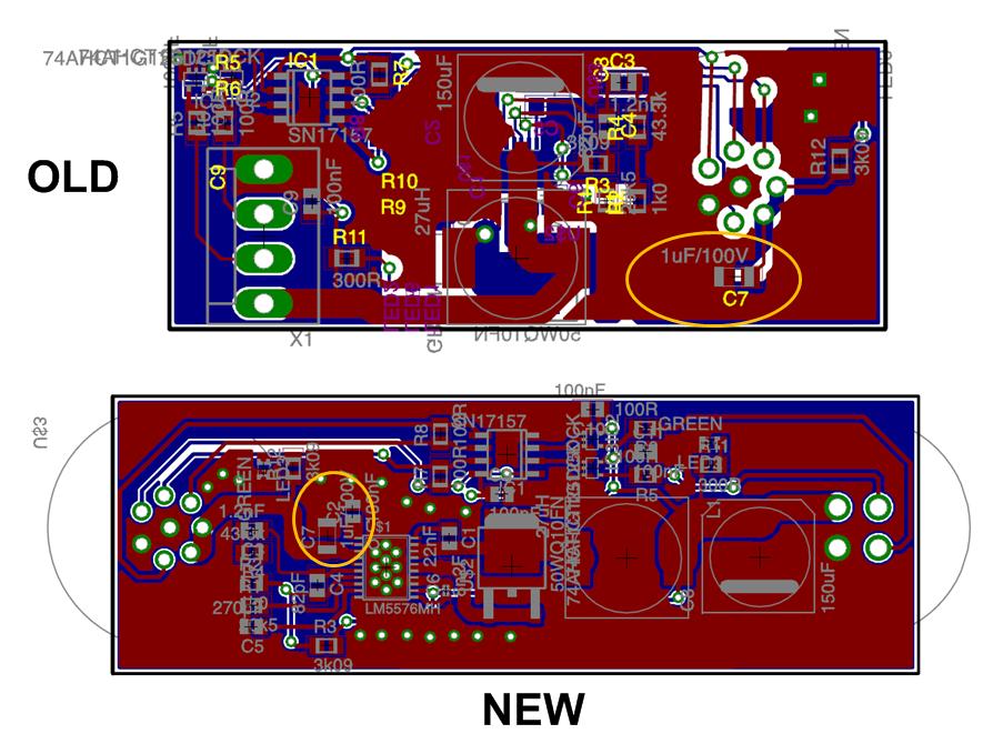
Hi, i have a problem with the LM5576 system i have put together based on a webbench design.   Attached is the circuit diagram

4532.sw_pixel_over_cat5_v3_4pin_kk.pdf

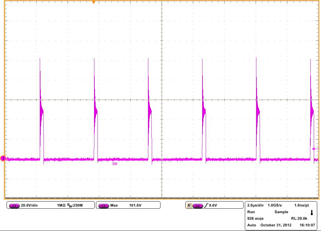
This runs, but when it a short or higher load is placed on the output, the circuit destroys itself..  A fuse on the input blows,  and the device itself is damaged, so it does'nt not work any more.

I thought that the LM5576 had short circuit protection but it does not work for me?

  • Just to add to this, the input voltage is 48VDC.

  • Hi Andrew, 

    Thank you for the schematic. Would it be possible for you to also share your board layout?

    Also, do you have an oscilloscope to capture the input voltage as you are overloading the output?

    Regards, 
    Denislav 

  • Hi, No sorry i do not have a scope trace of the input when it overloads.     I can tell you however, that it blows a 600mA fuse when it goes.  My inital guess is that something is going short circuit..   What i know is that it remains reletively stable when it is delivering up to 1100mA @ 5V, there is about 100mv of ripple, and a little bit of noise, but nothing that is problematic.

    I have attacehd my pcb layout.   

    I have looked at the pcb layout and i am wondering how much of this could be a problem.  I have reworked the pcb design and i'm about to try somethign different, with a layout that is only single sided, with a ground plan on the back. Hopefully that will be 

    Old PCB

    5226.sw_pixel_over_cat5_v3_4pin_kk_v2.pdf

    New PCB

    0081.sw_pixel_over_cat5_v3_4pin_kk_v3.pdf

    I would be very interested to know how the PCB layout can affect the design so much?

    Replacing teh LM5576 after the failure, solves the problem, so it looks like it is failing..

  • Hi Andrew, 

    Thank you for the layout files. 

    Bad board layout (i.e. improper input cap placement on a buck converter) can cause large spikes on the switch node due to parasitic inductance in the high di/dt loop. These spikes can go over the abs max on the SW pin (depending on how fast the switch transition is and how much parasitic inductance there is) and damage the device. I don't think this is happening in your case. Your input voltage is way below the operating maximum and the placement of the power stage components looks OK to me.

    I will review the schematic and layout again in more detail later today and provide some more feedback. It would be beneficial to probe the input voltage, sw node, and output voltage with a scope and get an idea of the device operation. 

    Questions:

    How fast is the input voltage ramp up time? Is the input to the LM5576 hot plugged?

    Also, after you replace the unit does it ever fail again?

    Regards, 

    Denislav

  • The input rise time according to the datasheet is 800ms.

    Hot plugging the LM5576 doesnt cause it to fail.  The failure comes when applying a load of more than about 1A.  

    Yes, if i repalce the LM5576 with a new one,   i can get a repeat failure by shorting the output.

    Is is possible i have a bad tube of ICS?

  • Hi Andrew, 

    What is the inductor Idc and Isat rating?

    One possibility is that the inductor may be saturating under the output short circuit condition and damaging the integrated FET. The typical short circuit current limit of the LM5576 is 4.2A (it is a 3A part). 

    Regards, 

    Denislav

  •  THe inductor i'm using is a bournes SRR1210-270M ( as suggested by the workbench ).    Its Isat is 4.2A, there is no Idc rating.  The Irms is 5.0A

    http://www.bourns.com/data/global/pdfs/SRR1210.pdf

  • Hi Andrew, 

    I modified an evaluation board with your values and tested your design in the lab. The short circuit protection worked well and I did not observe any failures with hard short on the output. 

    I'm sorry that I misunderstood your earlier post. I reviewed your new board layout earlier and mentioned that it looks good. However, you are probably getting the failures on the old layout, which is not optimized. In particular, the capacitor C7 (the input cap) is very far away from the IC and also sits on a different layer than the IC. The input capacitor is not doing much when sitting that far away from the IC. Your new layout is much better.

    Because of the cap placement there is a lot of parasitic inductance in the switching current loop.This will result in a lot of noise and high switching spikes. If you probe the switch node with a scope I am sure that you will see quite a bit of noise. This will get worse as you increase the output current because the di/dt gets larger.

    The good news is that your new board layout looks very similar to the evaluation board and the evaluation board with your BOM behaves normally. Here is a link to the evaluation board app note: http://www.ti.com/lit/ug/snva210a/snva210a.pdf for more details on that layout.

    I think this verifies that the list of components is good and it must be a layout issue. I believe that the design will work properly on your new board layout. If you would like, you can also try the components you got on an evaluation board and verify it with the rest of your system. 

    Regards, 

    Denislav

  • Thankyou very much for doing the testing..  I 'borrowed' the layout from the the eval board, so thats why it looks so similar.   I am just in teh process of building up the new layout and will let you know how it goes.

  • Andrew, 

    I ran another experiment on the evaluation board, again to point to the issue with the old layout. Here is a picture of this, the cap is sitting on the two input wires:

    I placed the input capacitor farther away to replicate your old layout. Here is a scope shot of the switch node with the cap "close" and the cap "far" from the IC. Notice the increase in ringing and spike amplitude.

    cap "close":

    cap "far": 

    Finally, I shorted the output of the regulator with the input capacitor being far away and the device got damaged just like in your case. 

    I think this is another confirmation that the layout has to be modified.

    Regards, 
    Denislav 

  • Firstly i'm totally blown away by the level of support that i've had.   You've gone way past what i could have dreamed for. Thanks so much.

    I've jsut run some tests imilar to what you dod with the Cap on PCB and i get a spike that is a bit higher than yours. at about 112V.    

    We are just manufacturing PCB#2, and i hope to give it a try shortly, and i'll let you know how we go.


  • Andrew, 

    Thank you for the positive feedback. I will pass it along to the whole SIMPLE SWITCHER apps team. We all try hard to support the field as much as possible and this sort of interaction helps us make better products and also write better datasheets and app notes. Thank YOU for using E2E. 

    Let us know how the new board works.

    Regards, 

    Denislav

  • Moving the input capacitor made all the difference.  Its all working very nicely now.  

  • Andrew, 

    Great! Thank you for the update. I am glad it works.

    Regards, 

    Denislav