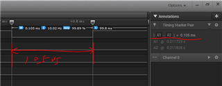
In MCU domain, cortex r5f calls CSL_ Armr5mpucfgregion writes the memory protection register to realize the memory protection function. The execution time of this function is 105us.
I don't think this time is correct. Ask experts to help me.
FIgure 1
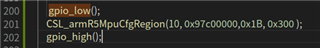
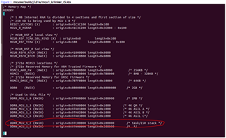
figure 2
/root/psdk_07_03/pdk_jacinto_07_03_00_29/packages/ti/csl/arch/r5/src/csl_arm_r5_mpu.asm
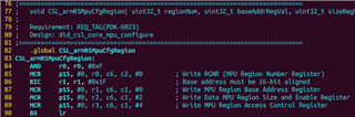
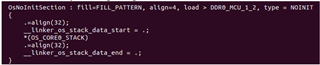
figure 3