This thread has been locked.

If you have a related question, please click the "Ask a related question" button in the top right corner. The newly created question will be automatically linked to this question.

DRA829V: DDR4 pad drive registers

Part Number: DRA829V
Other Parts Discussed in Thread: DRA829

We are verifying our LPDDR4 interface using Micron MT53D1024M32D4DT-046 at 3733-Mbps speed grade and see some issues with the quality of our data writes.

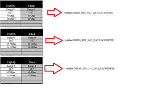
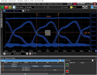
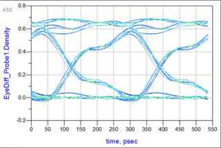
Data WRITE eye. DRA829 driving, measured at Micron chip.

Meanwhile. our Data READ eye looks much better. (Micron chip transmitting, measured at DRA829). 

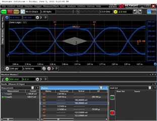
The above images are shown using standard 40-ohm termination settings.

I have tried adjusting these values to dozens of different combinations. None of them seem to have more than a marginal effect on the signal integrity. The same general shape persists. 

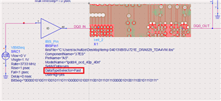
I was able to get an ADS simulation to show similar results, but only by changing the DataTypeSelector to "FAST", which also looks like it had some effect on the package RLC values

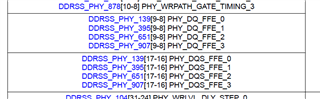
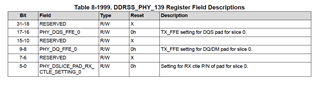
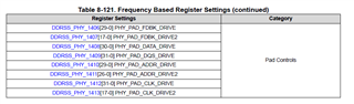
Reading through the TRM, I noticed this batch of registers which are referred to as Pad Controls. 

However, the TRM isn't really helpful in the register description.

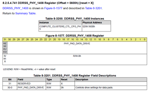
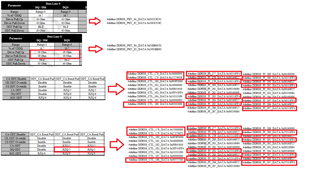
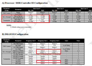
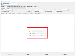
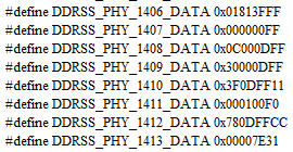
I do notice that when I adjust the termination settings in the J7 DDRSS Register Configuration spreadsheet, only the pad drive settings for the clock change with adjustments to the Address/Command termination configuration. Changing data/dqs termination does not appear to have any effect PHY_1408 register at all. Here is what we currently set the values to, based on the spreadsheet results.

I would like more information on what the registers are for, if they need to be adjusted from shown, a more detailed description of the bits etc. It's also possible I'm using an outdated version of the spreadsheet? It is dated August 4th, 2020 Rev 0.5.0. I attached it below.

I would check and compare it to our EVM board, but the vias are all backdrilled and there is no access to any of the DDR4 signals for probing. I am curious if/how TI managed to verify this interface on the EVM (interposer?). 

Jacinto7_DDRSS_RegConfigTool_evan_modified_tune.xlsm

  • Hi Evan,

    Regarding the XLS revision, the latest revision (v0.6.0) of the XLS tool was just released on TI.com: https://www.ti.com/lit/pdf/spracu8

    However, the only functionality surrounding  IO settings that changed between revision  0.5.0 and 0.6.0 of the XLS tool was related to the PHY_PAD_FDBK_DRIVE and PHY_PAD_FDBK_DRIVE2 settings (PHY_1406 and PHY_1407).

    The values you have boxed in red of section A of the IOControl tab of the XLS will impact the phy_dq_tsel_select and phy_dqs_tsel_select parameters (ex: see registers DDRSS_PHY_84 and DDRSS_PHY_85 for byte lane 0). The DQ ODT from section B of the IOControl tab of the XLS will impact the controller / PI MR11 parameters (CTL_178, CTL_179, CTL_186, PI_277, PI_279, PI_283, PI_285, PI_289, PI_291, PI_295, PI_297).

    Can you confirm whether these change when you modify these parameters? If they do not change, you may need to ensure that the XLS has auto calculation turned on for formulas (see section 4.1.2 of SPRACU8 , above link, for more information). 

    Regards,
    Kevin

  • I can confirm that changing those termination settings do change the registers. This is true with both versions of the spreadsheet.

    The reason my interest is in the pad drive settings is because I am seeing the pad drive settings for the clock adjust with changes to clock termination:

    Whereas I do not see any changes to DDRSS_PHY_1408 (data) or PHY_1409 (dqs) when i adjust dq/dqs drive strength/termination settings.

    This made me curious since termination adjustments to my clock showed significant improvement. (See image below. I had initially set everything to 80 ohms to account for the T-Split since it is a dual-die package but it turns out that wasn't neccessary. ended up backing out to 40 ohm drive strength with RZQ/5 termination). But termination adjustments to my DQ/DQS showed virtually no improvement in signal quality. 

    I wouldn't expect the data/dqs lines to need much termination adjusting since it's all just point-to-point routing. That's why I'm concerned there's some other drive setting(s) specific to the DRA829 EMIF implementation that are being missed (we had a similar issue with the SGMII interface you can see here: https://e2e.ti.com/support/processors-group/processors/f/processors-forum/1019099/tda4vm-sgmii-de-emphasis-register/) .

    The micron part doesn't seem to have an issue driving a clean signal back to the processor, so it seems unlikely to be a layout issue.

    Thanks,

    Evan

  • Hi Evan,

    Is this issue still present? You mentioned that you were able to reproduce the issue in simulations. Did changing the IO settings in simulations improve the issue?

    Regarding the register mapping, have you tried something other than 40 and 48 Ohm to observe the impact on the waveform? Although you would probably not want to use something like 120 or 240 Ohm, this could at least give you confidence that the tool is in fact changing the drive strength. Also, you could try changing  just drive strength and leave the DRAM ODT set to 40 Ohm to see if this changes the amplitude / signal quality.

    Thanks,
    Kevin 

  • Hi Kevin,

    I have tried a number of different termination settings (both at the receiver and transmitter) without seeing any significant improvements in waveform quality. Results shown in the previous posts were the best I could get from adjusting the termination settings in terms of vmargin and tmargin, but they were all more or less the same waveform shape.

    That being said, I did see these registers as I was digging through the TRM.

    example register field description for data slice 0:

    It looks like there is RX and TX equalization on the PHY for the DQ and DQS signals. This looks much more promising than the pad drive stuff I was looking at before. All of these registers are initialized to 0 using the XLS tool. 

    Since the TRM doesn't really mention these anywhere - and I don't have documentation for the Cadence Denali IP - I don't know exactly what these do. I'm hoping this is providing four levels of either pre-emphasis or de-emphasis on the TX. The CTLE on the RX looks to be unnecessary in our current implementation.

    To simulate any of these equalization settings would require IBIS-AMI files which I don't think were ever provided by TI for the DDR interface (I've only seen the regular IBIS files). 

    If TI could provide any further description on these FFE and CTLE settings that would be great. 

    Haven't had a chance yet to get the high speed probe adapters re-attached to one of my boards and taken to our other facility which has the high speed scope. When I get a chance I'll run through all four values for the FFE and provide screenshots of what they do to the eye diagram.

    Thanks,

    Evan