Other Parts Discussed in Thread: AM5728, ADC3660, MATHLIB
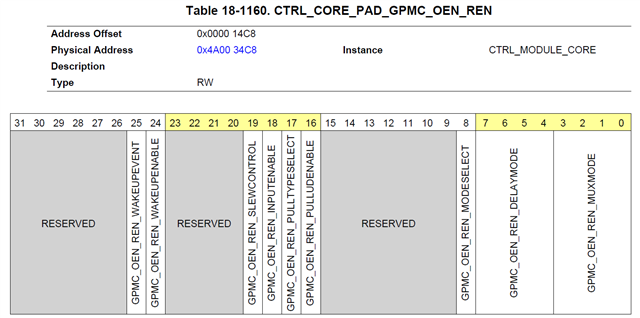
I am porting a working AM5728 application to a AM5706. Some of my GPIO's had to be moved in the transition so I have to change some control module register definitions. I am not sure how to determine these values and the existing code isn't giving me enough to go on. Is there some documentation above the TRM that will help? I was hoping the PINMUX tool might be of help but that doesn't seem to have what I am looking for. Also wondering where "PILLUP" came from since I am thinking it would be "PULLUP".
Here is what that section of code looks like in the existing 5728 project. I can make sense of the "Port and pin number mask for GPIO Load pin" section. Its the "Control module register definitions" that throw me:
#include <ti/drv/gpio/soc/GPIO_v1.h>
#include <stdio.h>
#include <ti/csl/soc.h>
#include <ti/csl/hw_types.h>
#include "GPIO_config.h"
#include "ControlLoops.h"
#include "PWM_Config.h"
/* Port and pin number mask for GPIO Load pin.
Bits 7-0: Pin number and Bits 15-8: Port number */
#define GPIO_LED_GREEN_PIN (0x0218)
#define GPIO_LED_RED_PIN (0x0219)
#define GPIO_TP48_PIN (0x021B)
#define GPIO_TP49_PIN (0x021C)
#define GPIO_EXT_SONICS_PIN (0x0504) //GPIO5_4, G13, I
#define GPIO_PWR_OL_PIN (0x0505) //GPIO5_5, J11, I
#define GPIO_VOLT_OL_PIN (0x0506) //GPIO5_6, E12, I
#define GPIO_CURR_OL_PIN (0x0507) //GPIO5_7, F13, I
#define GPIO_TEMP_OL_PIN (0x0508) //GPIO5_8, C12, I
#define GPIO_TEST_SW_PIN (0x0509) //GPIO5_9, D12, I
#define GPIO_EN_SONICS_PIN (0x060E)
#define GPIO_RESET_PS_PIN (0x060F)
#define GPIO_ADC3660_RESET_PIN (0x0610)
/* control module register definitions */
#define CTRL_CORE_PAD_GPMC_OEN_REN (0xC8U) //GPIO2_24, O
#define CTRL_CORE_PAD_GPMC_OEN_REN_PILLUP (0x10000 | 0x0E)
#define CTRL_CORE_PAD_GPMC_WEN (0xCCU) //GPIO2_25, O
#define CTRL_CORE_PAD_GPMC_WEN_PILLUP (0x10000 | 0x0E)
#define CTRL_CORE_PAD_GPMC_BEN1 (0xD4U) //GPIO2_27, O
#define CTRL_CORE_PAD_GPMC_BEN1_PILLUP (0x20000 | 0x0E)
#define CTRL_CORE_PAD_GPMC_WAIT0 (0xD8U) //GPIO2_28, O
#define CTRL_CORE_PAD_GPMC_WAIT0_PILLUP (0x20000 | 0x0E)
#define CTRL_CORE_PAD_MCASP1_AXR2 (0x2BCU) //GPIO5_4, I
#define CTRL_CORE_PAD_MCASP1_AXR2_PILLUP (0x50000 | 0x0E)
#define CTRL_CORE_PAD_MCASP1_AXR3 (0x2C0U) //GPIO5_5, I
#define CTRL_CORE_PAD_MCASP1_AXR3_PILLUP (0x50000 | 0x0E)
#define CTRL_CORE_PAD_MCASP1_AXR4 (0x2C4U) //GPIO5_6, I
#define CTRL_CORE_PAD_MCASP1_AXR4_PILLUP (0x50000 | 0x0E)
#define CTRL_CORE_PAD_MCASP1_AXR5 (0x2C8U) //GPIO5_7, I
#define CTRL_CORE_PAD_MCASP1_AXR5_PILLUP (0x50000 | 0x0E)
#define CTRL_CORE_PAD_MCASP1_AXR6 (0x2CCU) //GPIO5_8, I
#define CTRL_CORE_PAD_MCASP1_AXR6_PILLUP (0x50000 | 0x0E)
#define CTRL_CORE_PAD_MCASP1_AXR7 (0x2D0U) //GPIO5_9, I
#define CTRL_CORE_PAD_MCASP1_AXR7_PILLUP (0x70000 | 0x0E)
#define CTRL_CORE_PAD_GPIO6_14 (0x288U) //GPIO6_14, O
#define CTRL_CORE_PAD_GPIO6_14_PILLUP (0x10000 | 0x0E)
#define CTRL_CORE_PAD_GPIO6_15 (0x28CU) //GPIO6_15, O
#define CTRL_CORE_PAD_GPIO6_15_PILLUP (0x30000 | 0x0E)
#define CTRL_CORE_PAD_GPIO6_16 (0x290U) //GPIO6_16, O
#define CTRL_CORE_PAD_GPIO6_16_PILLUP (0x30000 | 0x0E)
/* GPIO Driver board specific pin configuration structure */
GPIO_PinConfig gpioPinConfigs[] = {
/* Output pin : GPIO2_24 Green Led */
GPIO_LED_GREEN_PIN | GPIO_CFG_OUTPUT,
/* Output pin : GPIO2_25 Red Led */
GPIO_LED_RED_PIN | GPIO_CFG_OUTPUT,
/* Output pin : GPIO2_27 Test Point 48 */
GPIO_TP48_PIN | GPIO_CFG_OUTPUT,
/* Output pin : GPIO2_28 Test Point 49 */
GPIO_TP49_PIN | GPIO_CFG_OUTPUT,
/* Input pin : GPIO5_4, external sonics */
GPIO_EXT_SONICS_PIN | GPIO_CFG_INPUT,
/* Input pin : GPIO5_5, power overload */
GPIO_PWR_OL_PIN | GPIO_CFG_INPUT,
/* Input pin : GPIO5_6, voltage overload */
GPIO_VOLT_OL_PIN | GPIO_CFG_INPUT,
/* Input pin : GPIO5_7, current overload */
GPIO_CURR_OL_PIN | GPIO_CFG_INPUT,
/* Input pin : GPIO5_8, temperate overload */
GPIO_TEMP_OL_PIN | GPIO_CFG_INPUT,
/* Input pin : GPIO5_9, test switch */
GPIO_TEST_SW_PIN | GPIO_CFG_INPUT,
/* Output pin : GPIO6_14 to reset sonics power supply */
GPIO_EN_SONICS_PIN | GPIO_CFG_OUTPUT,
/* Output pin : GPIO6_15 to enable sonics */
GPIO_RESET_PS_PIN | GPIO_CFG_OUTPUT,
/* Output pin : GPIO6_16 to reset ADC3660 */
GPIO_ADC3660_RESET_PIN | GPIO_CFG_OUTPUT
};