This thread has been locked.

If you have a related question, please click the "Ask a related question" button in the top right corner. The newly created question will be automatically linked to this question.

[FAQ] PRU_ICSSG: How to check and set PRU Core Frequency in CCS?

Other Parts Discussed in Thread: SYSCONFIG

I am using a processor with PRU_ICSSG (AM24x, AM64x, AM65x). I am using Code Composer Studio (CCS) to connect to my processor. How do I check what frequency the PRU cores are running at? How do I change the PRU core frequency?

Note: these steps document how to use CCS to set PRU core frequency. CCS is useful when developing and debugging PRU applications. However, different steps will be required to set PRU clock frequency in production code where the PRU is initialized by a Linux, RTOS, or bare metal core.

Setting PRU core frequency from Linux: Reference [FAQ] PRU_ICSSG: How to check and set PRU Core Frequency in Linux?

Setting PRU core frequency from RTOS or bare metal: Use the SOC driver in MCU+ SDK. In MCU+ SDK documentation, reference "SOC Peripheral Drivers" > "SOC". Selecting a specific frequency in PRU-ICSS module in SysConfig adds auto-generated code to call the “SOC_moduleSetClockFrequency” API during initialization. If PRU-ICSS clock frequency needs to be changed later during run-time, the same API can be used again. Note that AM24x/AM64x SysConfig for SDK 8.0 and earlier only give options for clock frequencies 200MHz - 250MHz. AM24x/AM64x SysConfig for SDK 8.1 onwards give the full range of ICSSG clock frequencies from 200MHz - 333MHz (1GHz / 3)

  • This response will cover the general steps. Later responses will give specific examples.

    Where does the ICSSG core clock come from?

    For information about how PRU_ICSSG clocks are connected to the rest of the processor, reference the Technical Reference Manual (TRM) of the processor. Start with TRM section "PRU_ICSSG Integration", section "PRU_ICSSG Power and Clock Management", and table "PRU_ICSSG Clocks"

    The actual CORE_CLOCK that is used within an ICSSG is selected from either ICSSGn_CORE_CLK or ICSSGn_ICLK (250MHz, synchronized to interface clock). CORE_CLOCK is selected with register ICSSG_CORE_SYNC_REG, bit CORE_VBUSP_SYNC_EN.

    ICSSGn_CORE_CLK can be selected from different system clocks, depending on the device. ICSSGn_CORE_CLK is selected with register CTRLMMR_ICSSGx_CLKSEL, bit CORE_CLKSEL.

    When are the system clocks configured?

    There are different methods to initialize the EVM in CCS. This FAQ will assume you are following the steps at [FAQ] AM64x / AM24x: How to use Code Composer Studio (CCS) to connect to PRU_ICSSG?

    For AM24x/AM64x SDK 8.1 and earlier, the OPSI SBL NULL initialization binary does not enable PRU clocks. So the PLL output clock frequencies must be modified in the DMSC GEL script that executes when CCS connects to the processor's DMSC.

    TODO: Does this method apply to AM65x processors?

    TODO: Is there generic guidance for how a customer would find this DMSC GEL file across different processors?

    How do I check the System Clock Frequencies? 

    A GEL script is provided for checking the PLL configurations. The script can be executed from R5F0_0 or DMSC. To execute the script, connect to the desired core and execute: Scripts->PLL Configuration->Get PLL Configurations->Get_All_PLL_Configurations. The output from the GEL script can be used to calculate the PLL output frequencies. Please see the TRM table "PLLTS16FFCLAFRACF Output Clocks" for details on how the PLL output frequencies are calculated.

  • AM64x example: 

    ICSSGn_CORE_CLK selects between MAIN_PLL2_HSDIV0_CLKOUT (225MHz, 300MHz) or MAIN_PLL0_HSDIV9_CLKOUT (200MHz, 250MHz, 333MHz i.e. 1GHz / 3).

    Let's say we want to configure ICSSG1 to 250MHz.

    Checking the current PRU Core Clock Frequency

    The settings for the clock muxes shown in the TRM ICSSG1 integration diagram are configured via these registers:

    ICSSG1, CTRLMMR_ICSSG1_CLKSEL   :   4300 8044h
    
    ICSSG1, ICSSG_CORE_SYNC_REG     :   300A 603Ch

    These registers can be observed or modified in a CCS Memory Window. Connect to an R5 core. If the Memory Browser is not visible, open it with View > Memory Browser. Now you can navigate to different areas of memory by typing in the hex address that you want to view.

    From CCS Memory Window:

    0x40308044 = 0x00000000 => ICSSG1_CORE_CLK
    
    0x300a603c = 0x00000000 => MAIN_PLL2_HSDIV0_CLKOUT

    So the ICSSG1 is currently using ICSSG1_CORE_CLK. And ICSSG1_CORE_CLK is coming from MAIN_PLL2_HSDIV0_CLKOUT.

    From Get_All_PLL_Configurations GEL script:

    MAIN_Cortex_R5_0_0: GEL Output: Base address: 0x00680000
    MAIN_Cortex_R5_0_0: GEL Output: PLL index: 0x00000002
    MAIN_Cortex_R5_0_0: GEL Output: PLL index register base: 0x00002000
    MAIN_Cortex_R5_0_0: GEL Output: Register: 0x00000020
    MAIN_Cortex_R5_0_0: GEL Output: Reference Divider is:     1
    MAIN_Cortex_R5_0_0: GEL Output: Feedback Divider is:      72
    MAIN_Cortex_R5_0_0: GEL Output: Fractional Multiplier is: 0
    MAIN_Cortex_R5_0_0: GEL Output: Output Divider #1 is:     1
    MAIN_Cortex_R5_0_0: GEL Output: Output Divider #2 is:     1
    MAIN_Cortex_R5_0_0: GEL Output: Number of hsdivs: 10
    MAIN_Cortex_R5_0_0: GEL Output: HSDIV #0's divider value is: 6
    MAIN_Cortex_R5_0_0: GEL Output: HSDIV #0's clkout_en: 1
    MAIN_Cortex_R5_0_0: GEL Output: HSDIV #1's divider value is: 1
    MAIN_Cortex_R5_0_0: GEL Output: HSDIV #1's clkout_en: 0
    MAIN_Cortex_R5_0_0: GEL Output: HSDIV #2's divider value is: 9
    MAIN_Cortex_R5_0_0: GEL Output: HSDIV #2's clkout_en: 1
    MAIN_Cortex_R5_0_0: GEL Output: HSDIV #3's divider value is: 6
    MAIN_Cortex_R5_0_0: GEL Output: HSDIV #3's clkout_en: 1
    MAIN_Cortex_R5_0_0: GEL Output: HSDIV #4's divider value is: 18
    MAIN_Cortex_R5_0_0: GEL Output: HSDIV #4's clkout_en: 1
    MAIN_Cortex_R5_0_0: GEL Output: HSDIV #5's divider value is: 8
    MAIN_Cortex_R5_0_0: GEL Output: HSDIV #5's clkout_en: 1
    MAIN_Cortex_R5_0_0: GEL Output: HSDIV #6's divider value is: 8
    MAIN_Cortex_R5_0_0: GEL Output: HSDIV #6's clkout_en: 1
    MAIN_Cortex_R5_0_0: GEL Output: HSDIV #7's divider value is: 18
    MAIN_Cortex_R5_0_0: GEL Output: HSDIV #7's clkout_en: 1
    MAIN_Cortex_R5_0_0: GEL Output: HSDIV #8's divider value is: 1
    MAIN_Cortex_R5_0_0: GEL Output: HSDIV #8's clkout_en: 0
    MAIN_Cortex_R5_0_0: GEL Output: HSDIV #9's divider value is: 5
    MAIN_Cortex_R5_0_0: GEL Output: HSDIV #9's clkout_en: 1
    MAIN_Cortex_R5_0_0: GEL Output: Parsed PLL configuration information.

    OSC: 25 MHz

    FOUTP = (25e6/1) * (72 + 0) / (1*1) = 1.8e9

    FOUTPOSTDIV = 1.8e9/6 = 300e6, 300 MHz

    So the ICSSG1 core clock is currently set to 300MHz.

    Changing the PRU core Clock Freqency 

    Where is the GEL file? 

    ccs_base\emulation\gel\AM64x\AM64x.gel --> OnTargetConnect() -->runs Set_All_PLL_OFC1(). Set_All_PLL_OFC1() is defined in ccs_base\emulation\gel\AM64x\AM64_PLL\AM64x_PLL_OFC1.gel.

    Set_All_PLL_OFC1() runs Setup(), which is defined in ccs_base\emulation\gel\AM64x\AM64_PLL\AM64x_PLL.gel. Setup() calls Program_PLL(). Since Clocking_Scheme = OFC1, then MAIN_PLL2_HSDIV0_CLKOUT divider is set by MAIN_PLL2_OFC1_HSDIV0_DIV_VAL, and MAIN_PLL0_HSDIV9_CLKOUT divider is set by MAIN_PLL0_OFC1_HSDIV9_DIV_VAL.

    If we check ccs_base\emulation\gel\AM64x\AM64_PLL\25MHz_HFOSC\AM64x_PLL_PARAMS_OFC1.gel, we see that
    MAIN_PLL2_OFC1_HSDIV0_DIV_VAL = 5 (Divide by 6)
    MAIN_PLL0_OFC1_HSDIV9_DIV_VAL = 2 (divide by 3)

    For PLL2, HSDIV0: 1800MHz divided by 6 gives 300MHz, which matches the output from the Get_All_PLL_Configurations GEL script.


    How do I change the PLL divider? 

    Let's say we want to use MAIN_PLL2_HSDIV0_CLKOUT, but have 225MHz clock instead of 300MHz clock. Then we would update ccs_base\emulation\gel\AM64x\AM64_PLL\25MHz_HFOSC\AM64x_PLL_PARAMS_OFC1.gel entry MAIN_PLL2_OFC1_HSDIV0_DIV_VAL to divide 1800MHz by 8 to get an output clock of 225MHz:

    #define MAIN_PLL2_OFC1_HSDIV0_DIV_VAL    7      //8


    How do I select a different clock source? 

    As a reminder, these are the ICSSG1 registers that select the clock going to the AM64x ICSSG1 cores:

    ICSSG1, CTRLMMR_ICSSG1_CLKSEL   :   4300 8044h
    
    ICSSG1, ICSSG_CORE_SYNC_REG     :   300A 603Ch

    Let's say we want to select 250MHz ICSSG1_ICLK instead of ICSSG1_CORE_CLK. Then we need to update register ICSSG_CORE_SYNC_REG, bit CORE_VBUSP_SYNC_EN from 0 to 1.

    Go to the Memory Browser and navigate to 0x300A603C. Verify that the 32 bit address you are looking at is the correct memory address by hovering your mouse over the 8 bytes until the address you are hovering over appears. Now you can edit the register value by double clicking on the address.

    The PRU core clock will now be supplied by the 250MHz interface clock.

    What if we want to run the PRU cores so there is exactly 3ns per PRU clock cycle? Then we need the 333MHz clock supplied from MAIN_PLL0_HSDIV9_CLKOUT.

    First, check that register ICSSG_CORE_SYNC_REG, bit CORE_VBUSP_SYNC_EN has a value of 0 (i.e., that we are using ICSSG1_CORE_CLK).

    Next, we need to write to CTRLMMR_ICSSG1_CLKSEL. However, the CTRLMMR registers are write protected. In order to write a new value into a CTRLMMR register, we need to unlock the kick register first. For more information, reference the TRM section "Kick Protection Registers".

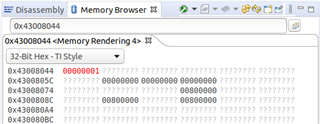
    There is a GEL script in CCS which can be used to unlock the MCU_CTRL_MMR registers. First, make sure you are connected to an R5 core. then go Scripts->Lock-Unlock->Unlock_Register, and enter the address to unlock: 0x43008044. Now you can navigate to 0x43008044 in the Memory Browser and update the CORE_CLKSEL bit. In this example, IEP_CLKSEL bits were already set to 0, and I left them unchanged.


    The PRU core clock will now be supplied by MAIN_PLL0_HSDIV9_CLKOUT. The default GEL script already sets MAIN_PLL0_HSDIV9_CLKOUT to 333MHz (1GHz/3, or exactly 3ns) as per section "Where is the GEL file?", so no GEL script updates are required. If you want to use a different frequency from MAIN_PLL0_HSDIV9_CLKOUT, you will need to update the PLL divider as described above.