Other Parts Discussed in Thread: DRA821
Hi
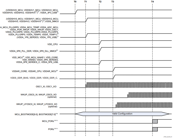
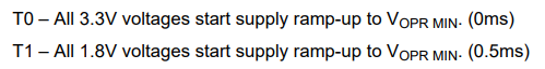
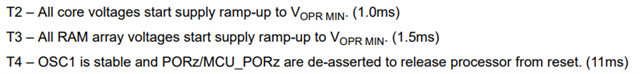
At DRA821 data sheet around p.99 "8.10.2.2/3 combined MCU and Main Domains Power- up/down Sequencing"
describes the TX (X: 0, 1, 2, 3, 4) as
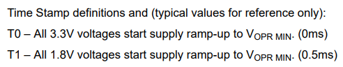
"Values shown are typical for PDNs combining MCU and Main voltage domains but could vary based upon PDN design. Time Stamp definitions and (typical values for reference only): "
Due to the lack of clear requirements on the DRA821 side, it is not possible to determine the design validity of the PMIC or the feasibility of the PMIC.
Please provide the specification of each Tx's Min/Max?
(For example,
T0:min x(ms)
max x(ms)
or
T0~T1: min x(ms)
max x(ms)