This thread has been locked.

If you have a related question, please click the "Ask a related question" button in the top right corner. The newly created question will be automatically linked to this question.

DRA829V: Decoupling cap placement

Part Number: DRA829V

HI All,

I have a question about the placement of the decoupling cap in J721E EVM BRD.

https://www.ti.com/tool/J721EXSOMXEVM 

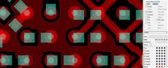
The EVM BRD (PROC078E8_BRD/PROC078E8A(001)_SCH) use the Via on pad for the capacitors on the bottom layer.

If we are not able to use this way to place those caps, is there any guideline or reference document for it?

Please kindly share your comment with us. 

Thank you.

  • No - we do not have sample layout of designs that do not support via in pad.  The PCB design goal should be to keep the inductance path as short as possible for the high frequency decoupling capacitors, especially on the high current/low voltage rails (CORE, CPU, etc).  Another decoupling capacitor option in addition to backside capacitors is to place decoupling on the top/SOC side, and have the power plane also near the top/SOC side.  This can help reduce total via length (reduced inductance) between the capacitor and the SoC.