This thread has been locked.

If you have a related question, please click the "Ask a related question" button in the top right corner. The newly created question will be automatically linked to this question.

66AK2H14: 66AK2H14 crashes after DDR3 access (ERROR -1202)

Part Number: 66AK2H14

Hi team, 

My customer encounters a very specific problem while using the 66AK2H14 on a custom board. 

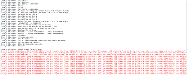
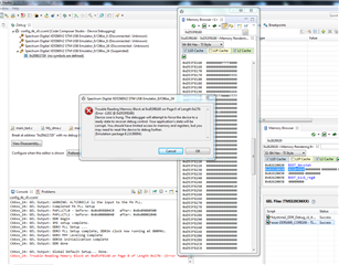
After connecting to the target, he runs the gel file, to initialize the SoC (very similar to the GEL by default on this version of CCSv910, ie log below). However, even if the DDR3 seems to be initialized properly, a DDR3 access (through memory browser or with a direct access through the ddr3A_memory_test () function for example) leads the CPU to crash

- emulator is XDS560V2STM and CCSv910

- CCS sends the error -1202 ie below. This error is not specified here https://software-dl.ti.com/ccs/esd/documents/ccs_debugging_jtag_connectivity_issues.html#device-hung

- JTAG tests prove a correct physical interconnection with the DDR.

- The supply voltage of both the CPU and the DDR has been tested and don't show any problem.

          -> How can a DDR access makes the CPU to crash ? 

          -> Do you have any explanation or recommendations on tests to be carried out ?

          -> I saw a very similar post here https://e2e.ti.com/support/processors-group/processors/f/processors-forum/1014972/66ak2g12-what-s-this-error-message-of-ccs-ddr-access-by-memory-browser/3751531?tisearch=e2e-sitesearch&keymatch=ERROR%201202#3751531 but has not been answered properly, have you found a solution since then? 

Regards,

Geoffrey

Error connecting to the target: (Error -1202 @ 0x6E) Device core is hung. The debugger will attempt to forced the device to a ready state and recovered debug control, but your application's state will be corrupt. You should have limited access to memory and registers, but you may need to reset the device to debug further.

  • Here are two gel files my customer used to initialize the SoC for a 100 MHz DDR input frequency. 

     Coral_4k_DDR1000_CORE100 -bb.gelCoral_4k_DDR1600_CORE100.gel  

    Geoffrey

  • Geoffrey,

    I understand that this problem is on the custom board.

    just to narrow down the problem, 

    Few quick questions here:-

    1. By any chance they have the "66AK2H14 - TI EVM " board? 

    2. Do they tested the standard gel file ? Able to initialize the DDR, establish the JTAG connection.

    3. Able to load the sample program into the "66AK2H14 - TI EVM" , through CCS and inbuilt emulator? Able to run and get the output successfully?

    4. If yes, Would you please confirm that the CPU does not crash in the TI -EVM?

    ---> These steps will help us in comparing the custom board with the EVM board and locate the problem.

    Regards

    Shankari G

  • Hi Shankari, 

    Yes they have this EVM and they were able to run the standard gel, then access the DDR with no problem.

    Is it normal that a DDR access leads to the crash of a MPU ? 

    Regards,

    Geoffrey

  • Geoffrey,

    Ok, Let us go one by one and narrow down, categorize whether it is a hardware or software problem ....

    Would you please post the following.

    1. Upload the gel file used for the TI-EVM. ( not the one used for the custom board... The one, from which they modified for custom board .i.e,  Coral_4k_DDR1000_CORE100 -bb.gelCoral_4k_DDR1600_CORE100.gel   )

    The gel file initializes both the ARM cores and DSP cores??

    2. The snapshot output of "test connection" using the ccxml file. ( for TI-k2HEVM )

    3. The snapshot output of "test connection" using the ccxml file. ( for custom board )

    4. The output log of the gel file ( TI-K2HEVM ). -

               4.a ARM gel separately

                4.b and DSP gel separately

    5. The output log of the gel file for the custom board ( Upload the full log, not the snapshot of the error portion )

    --

    Please refer to the video file, I have uploaded below. That will show, how to run the "test connection", load and run the gel etc.

    As I do not have K2H, I have demonstrated in K2E board. You can follow the same steps on K2H-TI-EVM

    1. test connectionhttps://e2e.ti.com/support/processors-group/processors/f/processors-forum/1064431/faq-66ak2e05-how-to-create-target-configuration-and-do-test-connection-on-k2e-evm

    2. Load and run the ARM gelhttps://e2e.ti.com/support/processors-group/processors/f/processors-forum/1064437/faq-66ak2e05-how-to-load-and-run-the-arm-gel-file-on-k2e-evm

    3. Load and run the DSP gel https://e2e.ti.com/support/processors-group/processors/f/processors-forum/1064433/faq-66ak2e05-how-to-load-and-run-the-dsp-gel-file-on-k2e-evm

    Regards

    Shankari G

  • Hi Shankari, 

    Please find the requested logs attached to this email.

    regards,

    Geoffrey

    Custom_board_DDR-PHYA_confgurationt_1000.txt
    C66xx_24: GEL Output: ********************************************************
    C66xx_24: GEL Output: PLL Control Register (PLLCR)
    C66xx_24: GEL Output: DDR3A_PLLCR:			0x000DC000 (Address: 0x02329018)
    C66xx_24: GEL Output: 	FRQSEL[19:18]:			PLL Reference clock ranges from 166MHz to 275MHz (3)
    C66xx_24: GEL Output: Note: PLL Reference Clock should be 1/4 of DDR data rate. (i.e. 400MHz -> 1600MTs)
    C66xx_24: GEL Output: ********************************************************
    
    C66xx_24: GEL Output: ********************************************************
    C66xx_24: GEL Output: DRAM Timing Parameters Register 0 (DTPR0)
    C66xx_24: GEL Output: DDR3A_DTPR0:			0x61117744 (Address: 0x02329048)
    C66xx_24: GEL Output: 	tRFC[31:26]:			Activate to Activate command delay (same bank) is 24 cycles
    C66xx_24: GEL Output: 	tRRD[25:22]:			Activate to Activate command delay (diff banks) is 4 cycles
    C66xx_24: GEL Output: 	tRAS[21:16]:			Activate to Precharge command delay is 17 cycles
    C66xx_24: GEL Output: 	tRCD[15:12]:			Activate to Read/Write (on activated row) command delay is 7 cycles
    C66xx_24: GEL Output: 	tRP[11:8]:			Precharge command period is 7 cycles
    C66xx_24: GEL Output: 	tWTR[7:4]:			Internal write to read command delay is 4 cycles
    C66xx_24: GEL Output: 	tRTP[3:0]:			Internal read to precharge command delay is 4 cycles
    C66xx_24: GEL Output: ********************************************************
    
    C66xx_24: GEL Output: ********************************************************
    C66xx_24: GEL Output: DRAM Timing Parameters Register 1 (DTPR1)
    C66xx_24: GEL Output: DDR3A_DTPR1:			0x32841240 (Address: 0x0232904C)
    C66xx_24: GEL Output: 	tWLO[29:26]:			Write leveling output delay is 12 cycles
    C66xx_24: GEL Output: 	tWLMRD[25:20]:			Min delay from write leveling mode to first DQS edge is 40 cycles
    C66xx_24: GEL Output: 	tRFC[19:11]:			Refresh to Refresh command delay is 130 cycles
    C66xx_24: GEL Output: 	tFAW[10:5]:			4-bank activate period is 18 cycles
    C66xx_24: GEL Output: 	tMOD[4:2]:			Load mode update delay is 12 cycles (0)
    C66xx_24: GEL Output: 	tMRD[1:0]:			Load mode cycle time is 0 cycles
    C66xx_24: GEL Output: ********************************************************
    
    C66xx_24: GEL Output: ********************************************************
    C66xx_24: GEL Output: DRAM Timing Parameters Register 2 (DTPR2)
    C66xx_24: GEL Output: DDR3A_DTPR2:			0x50023200 (Address: 0x02329050)
    C66xx_24: GEL Output: 	tCCD[31]:			Read to read and write to write command delay is 4 cycles (0)
    C66xx_24: GEL Output: 	tRTW[30]:			Read to write command delay is standard bus turn around delay +1 clock (1)
    C66xx_24: GEL Output: 	tRTODT[29]:			Read to ODT delay is 0, may come immediately after read post-amble (0)
    C66xx_24: GEL Output: 	tDLLK[28:19]:			DLL locking time is 512 cycles
    C66xx_24: GEL Output: 	tCKE[28:19]:			CKE minimum pulse width (tCKESR) is 4 cycles
    C66xx_24: GEL Output: 	tXP[14:10]:			Power down exit delay is 12 cycles
    C66xx_24: GEL Output: 	tXS[9:0]:			Self refresh exit delay is 512 cycles
    C66xx_24: GEL Output: ********************************************************
    C66xx_24: GEL Output: Mode Register 0 (MR0)
    C66xx_24: GEL Output: DDR3A_MR0:				0x00001830 (Address: 0x02329054)
    C66xx_24: GEL Output: 	PD[12]:				Fast power down exit (DLL on) (1)
    C66xx_24: GEL Output: 	WR[11:9]:			Write Recovery is 8 cycles (4)
    C66xx_24: GEL Output: 	CL[6:4,2]:			Reserved Value cycles (6)
    C66xx_24: GEL Output: ********************************************************
    
    C66xx_24: GEL Output: ********************************************************
    C66xx_24: GEL Output: Mode Register 1 (MR1)
    C66xx_24: GEL Output: DDR3A_MR1:				0x00000006 (Address: 0x02329058)
    C66xx_24: GEL Output: 	AL[4:3]:			AL Disabled (0)
    C66xx_24: GEL Output: 	RTT[9,6,2]:			ODT is RZQ/4 on SDRAM (1)
    C66xx_24: GEL Output: 	DIC[5,1]:			Output Drive is RZQ/7 on SDRAM (1)
    C66xx_24: GEL Output: 	DE[0]:				DLL Enabled on SDRAM (0)
    C66xx_24: GEL Output: ********************************************************
    
    C66xx_24: GEL Output: ********************************************************
    C66xx_24: GEL Output: Mode Register 2 (MR2)
    C66xx_24: GEL Output: DDR3A_MR2:				0x00000008 (Address: 0x0232905C)
    C66xx_24: GEL Output: 	RTTWR[10:9]:			Dynamic ODT is Disabled (0)
    C66xx_24: GEL Output: 	CWL[5:3]:			CAS Write Latency is 6 cycles (1)
    C66xx_24: GEL Output: 	SRT[7]:				Normal Operating Temperature Range (0)
    C66xx_24: GEL Output: 	ASR[6]:				Auto Self-Refresh Power Management Disabled (0)
    C66xx_24: GEL Output: 	PASR[2:0]:			Partial Array Self-Refresh is set to Full Array (0)
    C66xx_24: GEL Output: ********************************************************
    
    C66xx_24: GEL Output: ********************************************************
    C66xx_24: GEL Output: Impedance Control Register 1 (Address/Command/Control signals) (ZQ0CR1)
    C66xx_24: GEL Output: DDR3A_ZQ0CR1:			0x0001005D (Address: 0x02329184)
    C66xx_24: GEL Output: 	ZPROG-ODT[7:4]:			On-Die Termination is set to N/A (5)
    C66xx_24: GEL Output: 	ZPROG-ZO[3:0]:			Output Impedance is set to 34ohms (13)
    C66xx_24: GEL Output: ********************************************************
    
    C66xx_24: GEL Output: ********************************************************
    C66xx_24: GEL Output: Impedance Control Register 1 (Data Lanes 0-3) (ZQ1CR1)
    C66xx_24: GEL Output: DDR3A_ZQ1CR1:			0x0001005B (Address: 0x02329194)
    C66xx_24: GEL Output: 	ZPROG-ODT[7:4]:			On-Die Termination is set to 60ohms (5)
    C66xx_24: GEL Output: 	ZPROG-ZO[3:0]:			Output Impedance is set to 40ohms (11)
    C66xx_24: GEL Output: ********************************************************
    
    C66xx_24: GEL Output: ********************************************************
    C66xx_24: GEL Output: Impedance Control Register 1 (Data Lanes 4-7) (ZQ2CR1)
    C66xx_24: GEL Output: DDR3A_ZQ2CR1:			0x0001005B (Address: 0x023291A4)
    C66xx_24: GEL Output: 	ZPROG-ODT[7:4]:			On-Die Termination is set to 60ohms (5)
    C66xx_24: GEL Output: 	ZPROG-ZO[3:0]:			Output Impedance is set to 40ohms (11)
    C66xx_24: GEL Output: ********************************************************
    
    
    Custom_board_DDR-PHYA_confgurationt_1600.txt
    C66xx_24: GEL Output: ********************************************************
    C66xx_24: GEL Output: PLL Control Register (PLLCR)
    C66xx_24: GEL Output: DDR3A_PLLCR:			0x0001C000 (Address: 0x02329018)
    C66xx_24: GEL Output: 	FRQSEL[19:18]:			PLL Reference clock ranges from 335MHz to 533MHz (0)
    C66xx_24: GEL Output: Note: PLL Reference Clock should be 1/4 of DDR data rate. (i.e. 400MHz -> 1600MTs)
    C66xx_24: GEL Output: ********************************************************
    
    C66xx_24: GEL Output: ********************************************************
    C66xx_24: GEL Output: DRAM Timing Parameters Register 0 (DTPR0)
    C66xx_24: GEL Output: DDR3A_DTPR0:			0x9D5CCC66 (Address: 0x02329048)
    C66xx_24: GEL Output: 	tRFC[31:26]:			Activate to Activate command delay (same bank) is 39 cycles
    C66xx_24: GEL Output: 	tRRD[25:22]:			Activate to Activate command delay (diff banks) is 5 cycles
    C66xx_24: GEL Output: 	tRAS[21:16]:			Activate to Precharge command delay is 28 cycles
    C66xx_24: GEL Output: 	tRCD[15:12]:			Activate to Read/Write (on activated row) command delay is 12 cycles
    C66xx_24: GEL Output: 	tRP[11:8]:			Precharge command period is 12 cycles
    C66xx_24: GEL Output: 	tWTR[7:4]:			Internal write to read command delay is 6 cycles
    C66xx_24: GEL Output: 	tRTP[3:0]:			Internal read to precharge command delay is 6 cycles
    C66xx_24: GEL Output: ********************************************************
    
    C66xx_24: GEL Output: ********************************************************
    C66xx_24: GEL Output: DRAM Timing Parameters Register 1 (DTPR1)
    C66xx_24: GEL Output: DDR3A_DTPR1:			0x32868380 (Address: 0x0232904C)
    C66xx_24: GEL Output: 	tWLO[29:26]:			Write leveling output delay is 12 cycles
    C66xx_24: GEL Output: 	tWLMRD[25:20]:			Min delay from write leveling mode to first DQS edge is 40 cycles
    C66xx_24: GEL Output: 	tRFC[19:11]:			Refresh to Refresh command delay is 208 cycles
    C66xx_24: GEL Output: 	tFAW[10:5]:			4-bank activate period is 28 cycles
    C66xx_24: GEL Output: 	tMOD[4:2]:			Load mode update delay is 12 cycles (0)
    C66xx_24: GEL Output: 	tMRD[1:0]:			Load mode cycle time is 0 cycles
    C66xx_24: GEL Output: ********************************************************
    
    C66xx_24: GEL Output: ********************************************************
    C66xx_24: GEL Output: DRAM Timing Parameters Register 2 (DTPR2)
    C66xx_24: GEL Output: DDR3A_DTPR2:			0x5002D200 (Address: 0x02329050)
    C66xx_24: GEL Output: 	tCCD[31]:			Read to read and write to write command delay is 4 cycles (0)
    C66xx_24: GEL Output: 	tRTW[30]:			Read to write command delay is standard bus turn around delay +1 clock (1)
    C66xx_24: GEL Output: 	tRTODT[29]:			Read to ODT delay is 0, may come immediately after read post-amble (0)
    C66xx_24: GEL Output: 	tDLLK[28:19]:			DLL locking time is 512 cycles
    C66xx_24: GEL Output: 	tCKE[28:19]:			CKE minimum pulse width (tCKESR) is 5 cycles
    C66xx_24: GEL Output: 	tXP[14:10]:			Power down exit delay is 20 cycles
    C66xx_24: GEL Output: 	tXS[9:0]:			Self refresh exit delay is 512 cycles
    C66xx_24: GEL Output: ********************************************************
    C66xx_24: GEL Output: Mode Register 0 (MR0)
    C66xx_24: GEL Output: DDR3A_MR0:				0x00001C70 (Address: 0x02329054)
    C66xx_24: GEL Output: 	PD[12]:				Fast power down exit (DLL on) (1)
    C66xx_24: GEL Output: 	WR[11:9]:			Write Recovery is 12 cycles (6)
    C66xx_24: GEL Output: 	CL[6:4,2]:			11 cycles (14)
    C66xx_24: GEL Output: ********************************************************
    
    C66xx_24: GEL Output: ********************************************************
    C66xx_24: GEL Output: Mode Register 1 (MR1)
    C66xx_24: GEL Output: DDR3A_MR1:				0x00000006 (Address: 0x02329058)
    C66xx_24: GEL Output: 	AL[4:3]:			AL Disabled (0)
    C66xx_24: GEL Output: 	RTT[9,6,2]:			ODT is RZQ/4 on SDRAM (1)
    C66xx_24: GEL Output: 	DIC[5,1]:			Output Drive is RZQ/7 on SDRAM (1)
    C66xx_24: GEL Output: 	DE[0]:				DLL Enabled on SDRAM (0)
    C66xx_24: GEL Output: ********************************************************
    
    C66xx_24: GEL Output: ********************************************************
    C66xx_24: GEL Output: Mode Register 2 (MR2)
    C66xx_24: GEL Output: DDR3A_MR2:				0x00000018 (Address: 0x0232905C)
    C66xx_24: GEL Output: 	RTTWR[10:9]:			Dynamic ODT is Disabled (0)
    C66xx_24: GEL Output: 	CWL[5:3]:			CAS Write Latency is 8 cycles (3)
    C66xx_24: GEL Output: 	SRT[7]:				Normal Operating Temperature Range (0)
    C66xx_24: GEL Output: 	ASR[6]:				Auto Self-Refresh Power Management Disabled (0)
    C66xx_24: GEL Output: 	PASR[2:0]:			Partial Array Self-Refresh is set to Full Array (0)
    C66xx_24: GEL Output: ********************************************************
    
    C66xx_24: GEL Output: ********************************************************
    C66xx_24: GEL Output: Impedance Control Register 1 (Address/Command/Control signals) (ZQ0CR1)
    C66xx_24: GEL Output: DDR3A_ZQ0CR1:			0x0001005D (Address: 0x02329184)
    C66xx_24: GEL Output: 	ZPROG-ODT[7:4]:			On-Die Termination is set to N/A (5)
    C66xx_24: GEL Output: 	ZPROG-ZO[3:0]:			Output Impedance is set to 34ohms (13)
    C66xx_24: GEL Output: ********************************************************
    
    C66xx_24: GEL Output: ********************************************************
    C66xx_24: GEL Output: Impedance Control Register 1 (Data Lanes 0-3) (ZQ1CR1)
    C66xx_24: GEL Output: DDR3A_ZQ1CR1:			0x0001005B (Address: 0x02329194)
    C66xx_24: GEL Output: 	ZPROG-ODT[7:4]:			On-Die Termination is set to 60ohms (5)
    C66xx_24: GEL Output: 	ZPROG-ZO[3:0]:			Output Impedance is set to 40ohms (11)
    C66xx_24: GEL Output: ********************************************************
    
    C66xx_24: GEL Output: ********************************************************
    C66xx_24: GEL Output: Impedance Control Register 1 (Data Lanes 4-7) (ZQ2CR1)
    C66xx_24: GEL Output: DDR3A_ZQ2CR1:			0x0001005B (Address: 0x023291A4)
    C66xx_24: GEL Output: 	ZPROG-ODT[7:4]:			On-Die Termination is set to 60ohms (5)
    C66xx_24: GEL Output: 	ZPROG-ZO[3:0]:			Output Impedance is set to 40ohms (11)
    C66xx_24: GEL Output: ********************************************************
    
    
    Custom_board_DSP_GEL_1600.txt
    C66xx_24: GEL Output: Global Default Setup...
    C66xx_24: GEL Output: JCL modifcation, TCI6638K2K GEL file Ver is 1.70000005 
    C66xx_24: GEL Output: Detected PLL bypass disabled: SECCTL[BYPASS] = 0x00000000
    C66xx_24: GEL Output: (3a) PLLCTL = 0x00000040
    C66xx_24: GEL Output: (3b) PLLCTL = 0x00000040
    C66xx_24: GEL Output: (3c) Delay...
    C66xx_24: GEL Output: (4)PLLM[PLLM] = 0x00000017
    C66xx_24: GEL Output: MAINPLLCTL0 = 0x0B000000
    C66xx_24: GEL Output: (5) MAINPLLCTL0 = 0x0B000000
    C66xx_24: GEL Output: (5) MAINPLLCTL1 = 0x00000040
    C66xx_24: GEL Output: (6) MAINPLLCTL0 = 0x0B000000
    C66xx_24: GEL Output: (7) SECCTL = 0x00090000
    C66xx_24: GEL Output: (8a) Delay...
    C66xx_24: GEL Output: PLL1_DIV3 = 0x00008002
    C66xx_24: GEL Output: PLL1_DIV4 = 0x00008004
    C66xx_24: GEL Output: PLL1_DIV7 = 0x00000000
    C66xx_24: GEL Output: (8d/e) Delay...
    C66xx_24: GEL Output: (10) Delay...
    C66xx_24: GEL Output: (12) Delay...
    C66xx_24: GEL Output: (13) SECCTL = 0x00090000
    C66xx_24: GEL Output: (Delay...
    C66xx_24: GEL Output: (Delay...
    C66xx_24: GEL Output: (14) PLLCTL = 0x00000041
    C66xx_24: GEL Output: PLL has been configured (CLKIN * PLLM / PLLD / PLLOD = PLLOUT):
    C66xx_24: GEL Output: PLL has been configured (100.0 MHz * 24 / 1 / 2 = 1200.0 MHz)
    C66xx_24: GEL Output: Switching on ARM Core 0
    C66xx_24: GEL Output: Switching on ARM Core 1
    C66xx_24: GEL Output: Switching on ARM Core 2
    C66xx_24: GEL Output: Switching on ARM Core 3
    C66xx_24: GEL Output: ARM PLL has been configured (100.0 MHz * 28 / 2 = 1400.0 MHz)
    C66xx_24: GEL Output:  DISABLESTAT ---> 0x000007FF 
    C66xx_24: GEL Output: Power on all PSC modules and DSP domains... 
    C66xx_24: GEL Output: Power on all PSC modules and DSP domains... Done.
    C66xx_24: GEL Output: WARNING: ALTCORECLK is the input to the PA PLL.
    C66xx_24: GEL Output: Completed PA PLL Setup
    C66xx_24: GEL Output: PAPLLCTL0 - before: 0x0x09080500	 after: 0x0x09080500
    C66xx_24: GEL Output: PAPLLCTL1 - before: 0x0x00002040	 after: 0x0x00002040
    C66xx_24: GEL Output: DDR begin
    C66xx_24: GEL Output: XMC setup complete.
    C66xx_24: GEL Output: DDR3 PLL Setup ... 
    C66xx_24: GEL Output: DDR3 PLL Setup complete, DDR3A clock now running at 800MHz.
    C66xx_24: GEL Output: DDR3 PHY Leveling Complete 
    C66xx_24: GEL Output: DDR3A initialization complete 
    C66xx_24: GEL Output: DDR done
    
    C66xx_24: GEL Output: Global Default Setup... Done.
    
    Custom_board_DSP_GEL_1000.txt
    C66xx_24: GEL Output: Global Default Setup...
    C66xx_24: GEL Output: JCL modifcation, TCI6638K2K GEL file Ver is 1.70000005 
    C66xx_24: GEL Output: Detected PLL bypass disabled: SECCTL[BYPASS] = 0x00000000
    C66xx_24: GEL Output: (3a) PLLCTL = 0x00000040
    C66xx_24: GEL Output: (3b) PLLCTL = 0x00000040
    C66xx_24: GEL Output: (3c) Delay...
    C66xx_24: GEL Output: (4)PLLM[PLLM] = 0x00000017
    C66xx_24: GEL Output: MAINPLLCTL0 = 0x0B000000
    C66xx_24: GEL Output: (5) MAINPLLCTL0 = 0x0B000000
    C66xx_24: GEL Output: (5) MAINPLLCTL1 = 0x00000040
    C66xx_24: GEL Output: (6) MAINPLLCTL0 = 0x0B000000
    C66xx_24: GEL Output: (7) SECCTL = 0x00090000
    C66xx_24: GEL Output: (8a) Delay...
    C66xx_24: GEL Output: PLL1_DIV3 = 0x00008002
    C66xx_24: GEL Output: PLL1_DIV4 = 0x00008004
    C66xx_24: GEL Output: PLL1_DIV7 = 0x00000000
    C66xx_24: GEL Output: (8d/e) Delay...
    C66xx_24: GEL Output: (10) Delay...
    C66xx_24: GEL Output: (12) Delay...
    C66xx_24: GEL Output: (13) SECCTL = 0x00090000
    C66xx_24: GEL Output: (Delay...
    C66xx_24: GEL Output: (Delay...
    C66xx_24: GEL Output: (14) PLLCTL = 0x00000041
    C66xx_24: GEL Output: PLL has been configured (CLKIN * PLLM / PLLD / PLLOD = PLLOUT):
    C66xx_24: GEL Output: PLL has been configured (100.0 MHz * 24 / 1 / 2 = 1200.0 MHz)
    C66xx_24: GEL Output: Switching on ARM Core 0
    C66xx_24: GEL Output: Switching on ARM Core 1
    C66xx_24: GEL Output: Switching on ARM Core 2
    C66xx_24: GEL Output: Switching on ARM Core 3
    C66xx_24: GEL Output: ARM PLL has been configured (100.0 MHz * 28 / 2 = 1400.0 MHz)
    C66xx_24: GEL Output:  DISABLESTAT ---> 0x000007FF 
    C66xx_24: GEL Output: Power on all PSC modules and DSP domains... 
    C66xx_24: GEL Output: Power on all PSC modules and DSP domains... Done.
    C66xx_24: GEL Output: WARNING: ALTCORECLK is the input to the PA PLL.
    C66xx_24: GEL Output: Completed PA PLL Setup
    C66xx_24: GEL Output: PAPLLCTL0 - before: 0x0x098804C0	 after: 0x0x09080500
    C66xx_24: GEL Output: PAPLLCTL1 - before: 0x0x00000040	 after: 0x0x00002040
    C66xx_24: GEL Output: DDR begin
    C66xx_24: GEL Output: XMC setup complete.
    C66xx_24: GEL Output: DDR3 PLL Setup ... 
    C66xx_24: GEL Output: DDR3 PLL Setup complete, DDR3A clock now running at 500MHz.
    C66xx_24: GEL Output: DDR3 PHY Leveling Complete 
    C66xx_24: GEL Output: DDR3A initialization complete 
    C66xx_24: GEL Output: DDR done
    
    C66xx_24: GEL Output: Global Default Setup... Done.
    C66xx_24: GEL Output: Global Default Setup... Done.
    Custom_board_EMIF_confgurationt_1600.txt
    C66xx_24: GEL Output: ****************************************************************************************************************
    C66xx_24: GEL Output: ********************************************************
    C66xx_24: GEL Output: DDR SDRAM Configuration Register (SDCFG)
    C66xx_24: GEL Output: DDR3AEMIF_SDCFG:			0x6200CE62 (Address: 0x21010008)
    C66xx_24: GEL Output: 	SDRAM Type[31:29]:   		DDR3 (3)
    C66xx_24: GEL Output: 	SDRAM Drive[27:25]:  		RZQ/4 (1)
    C66xx_24: GEL Output: 	Dynamic ODT[23:22]:  		OFF (0)
    C66xx_24: GEL Output: 	CAS Write Latency[16:14]:	8 (3)
    C66xx_24: GEL Output: 	Data Bus Width[13:12]: 		64-bit (0)
    C66xx_24: GEL Output: 	CAS Latency[11:8]:		11 (14)
    C66xx_24: GEL Output: 	Banks per SDRAM[6:5]: 		8 (3)
    C66xx_24: GEL Output: 	Chip Select Setup[3]: 		DCE0# (0)
    C66xx_24: GEL Output: 	Page Size[1:0]:    		1024 word page (2)
    C66xx_24: GEL Output: ********************************************************
    
    C66xx_24: GEL Output: ********************************************************
    C66xx_24: GEL Output: SDRAM Refresh Control Register (SDRFC)
    C66xx_24: GEL Output: DDR3AEMIF_SDRFC:			0x00000C34 (Address: 0x21010010)
    C66xx_24: GEL Output: 	INITREF_DIS[31]:		Normal operation
    C66xx_24: GEL Output: 	REFRESH_RATE[15:0]:		3124 (REFRESH_RATE = Refresh period * DDR3 clock frequency.)
    C66xx_24: GEL Output: ********************************************************
    
    C66xx_24: GEL Output: ********************************************************
    C66xx_24: GEL Output: SDRAM Timing 1 Register (SDTIM1)
    C66xx_24: GEL Output: DDR3AEMIF_SDTIM1:			0x166C9865 (Address: 0x21010018)
    C66xx_24: GEL Output: 	T_WR[29:25]:			11 cycles (+1)
    C66xx_24: GEL Output: 	T_RAS[24:18]:			27 cycles (+1)
    C66xx_24: GEL Output: 	T_RC[17:10]:			38 cycles (+1)
    C66xx_24: GEL Output: 	T_RRD[9:4]:			6 cycles (+1)
    C66xx_24: GEL Output: 	T_WTR[3:0]:			5 cycles (+1)
    C66xx_24: GEL Output: ********************************************************
    
    C66xx_24: GEL Output: ********************************************************
    C66xx_24: GEL Output: SDRAM Timing 2 Register (SDTIM2)
    C66xx_24: GEL Output: DDR3AEMIF_SDTIM2:			0x00001D6B (Address: 0x2101001C)
    C66xx_24: GEL Output: 	T_RTW[12:10]:			7 cycles (+1)
    C66xx_24: GEL Output: 	T_RP[9:5]:			11 cycles (+1)
    C66xx_24: GEL Output: 	T_RCD[4:0]:			11 cycles (+1)
    C66xx_24: GEL Output: ********************************************************
    
    C66xx_24: GEL Output: ********************************************************
    C66xx_24: GEL Output: SDRAM Timing 3 Register (SDTIM3)
    C66xx_24: GEL Output: DDR3AEMIF_SDTIM3:			0x435DFF53 (Address: 0x21010020)
    C66xx_24: GEL Output: 	T_XP[31:28]:			4 cycles (+1)
    C66xx_24: GEL Output: 	T_XSNR[27:18]:			215 cycles (+1)
    C66xx_24: GEL Output: 	T_XSRD[17:8]:			511 cycles (+1)
    C66xx_24: GEL Output: 	T_RTP[7:4]:			5 cycles (+1)
    C66xx_24: GEL Output: 	T_CKE[3:0]:			3 cycles (+1)
    C66xx_24: GEL Output: ********************************************************
    
    C66xx_24: GEL Output: ********************************************************
    C66xx_24: GEL Output: SDRAM Timing 4 Register (SDTIM4)
    C66xx_24: GEL Output: 	DDR3AEMIF_SDTIM4:		0x543F0CFF (Address: 0x21010028)
    C66xx_24: GEL Output: 	T_CSTA[31:28]:			4 cycles (+1)
    C66xx_24: GEL Output: 	T_CKESR[27:24]:			3 cycles (+1)
    C66xx_24: GEL Output: 	ZQ_ZQCS[23:16]:			93 cycles (+1)
    C66xx_24: GEL Output: 	T_RFC[13:4]:			1013 cycles (+1)
    C66xx_24: GEL Output: 	T_RAS_MAX[3:0]:(should be 0xF)	3 cycles
    C66xx_24: GEL Output: ********************************************************
    
    C66xx_24: GEL Output: ********************************************************
    C66xx_24: GEL Output: SDRAM Output Impedance Calibration Configuration Register (ZQCFG)
    C66xx_24: GEL Output: 	DDR3AEMIF_ZQCFG:		0x70073200 (Address: 0x210100C8)
    C66xx_24: GEL Output: 	ZQ_CS1EN[31]:			ZQ calibration for Rank 2 is Disabled (0)
    C66xx_24: GEL Output: 	ZQ_CS0EN[31]:			ZQ calibration for Rank 1 is Enabled (1)
    C66xx_24: GEL Output: 	ZQ_DUALCALEN[29]:		Dual ZQ calibration is Enabled (1)
    C66xx_24: GEL Output: 	ZQ_SFEXITEN[28]:		ZQ calibration on self-refresh, Active power-down and precharge power-down exit is Enabled (1)
    C66xx_24: GEL Output: 	ZQ_ZQCL_MULT[18:16]:		7 cycles
    C66xx_24: GEL Output: 	ZQ_REFINTERVAL[15:0]:		Refresh periods between ZQCS commands is 12800 (+1)
    C66xx_24: GEL Output: ********************************************************
    C66xx_24: GEL Output: ****************************************************************************************************************
    
    
    Custom_board_EMIF_confgurationt_1000.txt
    C66xx_24: GEL Output: ****************************************************************************************************************
    C66xx_24: GEL Output: ********************************************************
    C66xx_24: GEL Output: DDR SDRAM Configuration Register (SDCFG)
    C66xx_24: GEL Output: DDR3AEMIF_SDCFG:			0x62004662 (Address: 0x21010008)
    C66xx_24: GEL Output: 	SDRAM Type[31:29]:   		DDR3 (3)
    C66xx_24: GEL Output: 	SDRAM Drive[27:25]:  		RZQ/4 (1)
    C66xx_24: GEL Output: 	Dynamic ODT[23:22]:  		OFF (0)
    C66xx_24: GEL Output: 	CAS Write Latency[16:14]:	6 (1)
    C66xx_24: GEL Output: 	Data Bus Width[13:12]: 		64-bit (0)
    C66xx_24: GEL Output: 	CAS Latency[11:8]:		7 (6)
    C66xx_24: GEL Output: 	Banks per SDRAM[6:5]: 		8 (3)
    C66xx_24: GEL Output: 	Chip Select Setup[3]: 		DCE0# (0)
    C66xx_24: GEL Output: 	Page Size[1:0]:    		1024 word page (2)
    C66xx_24: GEL Output: ********************************************************
    
    C66xx_24: GEL Output: ********************************************************
    C66xx_24: GEL Output: SDRAM Refresh Control Register (SDRFC)
    C66xx_24: GEL Output: DDR3AEMIF_SDRFC:			0x00000C34 (Address: 0x21010010)
    C66xx_24: GEL Output: 	INITREF_DIS[31]:		Normal operation
    C66xx_24: GEL Output: 	REFRESH_RATE[15:0]:		3124 (REFRESH_RATE = Refresh period * DDR3 clock frequency.)
    C66xx_24: GEL Output: ********************************************************
    
    C66xx_24: GEL Output: ********************************************************
    C66xx_24: GEL Output: SDRAM Timing 1 Register (SDTIM1)
    C66xx_24: GEL Output: DDR3AEMIF_SDTIM1:			0x0E405C43 (Address: 0x21010018)
    C66xx_24: GEL Output: 	T_WR[29:25]:			7 cycles (+1)
    C66xx_24: GEL Output: 	T_RAS[24:18]:			16 cycles (+1)
    C66xx_24: GEL Output: 	T_RC[17:10]:			23 cycles (+1)
    C66xx_24: GEL Output: 	T_RRD[9:4]:			4 cycles (+1)
    C66xx_24: GEL Output: 	T_WTR[3:0]:			3 cycles (+1)
    C66xx_24: GEL Output: ********************************************************
    
    C66xx_24: GEL Output: ********************************************************
    C66xx_24: GEL Output: SDRAM Timing 2 Register (SDTIM2)
    C66xx_24: GEL Output: DDR3AEMIF_SDTIM2:			0x00001CC6 (Address: 0x2101001C)
    C66xx_24: GEL Output: 	T_RTW[12:10]:			7 cycles (+1)
    C66xx_24: GEL Output: 	T_RP[9:5]:			6 cycles (+1)
    C66xx_24: GEL Output: 	T_RCD[4:0]:			6 cycles (+1)
    C66xx_24: GEL Output: ********************************************************
    
    C66xx_24: GEL Output: ********************************************************
    C66xx_24: GEL Output: SDRAM Timing 3 Register (SDTIM3)
    C66xx_24: GEL Output: DDR3AEMIF_SDTIM3:			0x2219FF32 (Address: 0x21010020)
    C66xx_24: GEL Output: 	T_XP[31:28]:			2 cycles (+1)
    C66xx_24: GEL Output: 	T_XSNR[27:18]:			134 cycles (+1)
    C66xx_24: GEL Output: 	T_XSRD[17:8]:			511 cycles (+1)
    C66xx_24: GEL Output: 	T_RTP[7:4]:			3 cycles (+1)
    C66xx_24: GEL Output: 	T_CKE[3:0]:			2 cycles (+1)
    C66xx_24: GEL Output: ********************************************************
    
    C66xx_24: GEL Output: ********************************************************
    C66xx_24: GEL Output: SDRAM Timing 4 Register (SDTIM4)
    C66xx_24: GEL Output: 	DDR3AEMIF_SDTIM4:		0x533F081F (Address: 0x21010028)
    C66xx_24: GEL Output: 	T_CSTA[31:28]:			2 cycles (+1)
    C66xx_24: GEL Output: 	T_CKESR[27:24]:			2 cycles (+1)
    C66xx_24: GEL Output: 	ZQ_ZQCS[23:16]:			25 cycles (+1)
    C66xx_24: GEL Output: 	T_RFC[13:4]:			1011 cycles (+1)
    C66xx_24: GEL Output: 	T_RAS_MAX[3:0]:(should be 0xF)	2 cycles
    C66xx_24: GEL Output: ********************************************************
    
    C66xx_24: GEL Output: ********************************************************
    C66xx_24: GEL Output: SDRAM Output Impedance Calibration Configuration Register (ZQCFG)
    C66xx_24: GEL Output: 	DDR3AEMIF_ZQCFG:		0x70073200 (Address: 0x210100C8)
    C66xx_24: GEL Output: 	ZQ_CS1EN[31]:			ZQ calibration for Rank 2 is Disabled (0)
    C66xx_24: GEL Output: 	ZQ_CS0EN[31]:			ZQ calibration for Rank 1 is Enabled (1)
    C66xx_24: GEL Output: 	ZQ_DUALCALEN[29]:		Dual ZQ calibration is Enabled (1)
    C66xx_24: GEL Output: 	ZQ_SFEXITEN[28]:		ZQ calibration on self-refresh, Active power-down and precharge power-down exit is Enabled (1)
    C66xx_24: GEL Output: 	ZQ_ZQCL_MULT[18:16]:		7 cycles
    C66xx_24: GEL Output: 	ZQ_REFINTERVAL[15:0]:		Refresh periods between ZQCS commands is 12800 (+1)
    C66xx_24: GEL Output: ********************************************************
    C66xx_24: GEL Output: ****************************************************************************************************************
    
    
    Custom_board_levelling_error_report_1000.txt
    C66xx_24: GEL Output: ********************************************************
    C66xx_24: GEL Output: Leveling Errors by Byte Lane:
    
    C66xx_24: GEL Output: Byte Lane 0:
    C66xx_24: GEL Output: 	DX0GSR2[6]:   WEERR has 		** No Error **
    C66xx_24: GEL Output: 	DX0GSR2[4]:   REERR has 		** No Error **
    C66xx_24: GEL Output: 	DX0GSR2[2]:   WDERR has 		** No Error **
    C66xx_24: GEL Output: 	DX0GSR2[0]:   RDERR has 		** No Error **
    C66xx_24: GEL Output: 	DX0GSR0[25]:   QSGERR on Rank1 has 	** No Error **
    C66xx_24: GEL Output: 	DX0GSR0[24]:   QSGERR on Rank0 has 	** No Error **
    C66xx_24: GEL Output: 	DX0GSR0[6]:    WLERR has 		** No Error **
    C66xx_24: GEL Output: Byte Lane 1:
    C66xx_24: GEL Output: 	DX1GSR2[6]:   WEERR has 		** No Error **
    C66xx_24: GEL Output: 	DX1GSR2[4]:   REERR has 		** No Error **
    C66xx_24: GEL Output: 	DX1GSR2[2]:   WDERR has 		** No Error **
    C66xx_24: GEL Output: 	DX1GSR2[0]:   RDERR has 		** No Error **
    C66xx_24: GEL Output: 	DX1GSR0[25]:   QSGERR on Rank1 has 	** No Error **
    C66xx_24: GEL Output: 	DX1GSR0[24]:   QSGERR on Rank0 has 	** No Error **
    C66xx_24: GEL Output: 	DX1GSR0[6]:    WLERR has 		** No Error **
    C66xx_24: GEL Output: Byte Lane 2:
    C66xx_24: GEL Output: 	DX2GSR2[6]:   WEERR has 		** No Error **
    C66xx_24: GEL Output: 	DX2GSR2[4]:   REERR has 		** No Error **
    C66xx_24: GEL Output: 	DX2GSR2[2]:   WDERR has 		** No Error **
    C66xx_24: GEL Output: 	DX2GSR2[0]:   RDERR has 		** No Error **
    C66xx_24: GEL Output: 	DX2GSR0[25]:   QSGERR on Rank1 has 	** No Error **
    C66xx_24: GEL Output: 	DX2GSR0[24]:   QSGERR on Rank0 has 	** No Error **
    C66xx_24: GEL Output: 	DX2GSR0[6]:    WLERR has 		** No Error **
    C66xx_24: GEL Output: Byte Lane 3:
    C66xx_24: GEL Output: 	DX3GSR2[6]:   WEERR has 		** No Error **
    C66xx_24: GEL Output: 	DX3GSR2[4]:   REERR has 		** No Error **
    C66xx_24: GEL Output: 	DX3GSR2[2]:   WDERR has 		** No Error **
    C66xx_24: GEL Output: 	DX3GSR2[0]:   RDERR has 		** No Error **
    C66xx_24: GEL Output: 	DX3GSR0[25]:   QSGERR on Rank1 has 	** No Error **
    C66xx_24: GEL Output: 	DX3GSR0[24]:   QSGERR on Rank0 has 	** No Error **
    C66xx_24: GEL Output: 	DX3GSR0[6]:    WLERR has 		** No Error **
    C66xx_24: GEL Output: Byte Lane 4:
    C66xx_24: GEL Output: 	DX4GSR2[6]:   WEERR has 		** No Error **
    C66xx_24: GEL Output: 	DX4GSR2[4]:   REERR has 		** No Error **
    C66xx_24: GEL Output: 	DX4GSR2[2]:   WDERR has 		** No Error **
    C66xx_24: GEL Output: 	DX4GSR2[0]:   RDERR has 		** No Error **
    C66xx_24: GEL Output: 	DX4GSR0[25]:   QSGERR on Rank1 has 	** No Error **
    C66xx_24: GEL Output: 	DX4GSR0[24]:   QSGERR on Rank0 has 	** No Error **
    C66xx_24: GEL Output: 	DX4GSR0[6]:    WLERR has 		** No Error **
    C66xx_24: GEL Output: Byte Lane 5:
    C66xx_24: GEL Output: 	DX5GSR2[6]:   WEERR has 		** No Error **
    C66xx_24: GEL Output: 	DX5GSR2[4]:   REERR has 		** No Error **
    C66xx_24: GEL Output: 	DX5GSR2[2]:   WDERR has 		** No Error **
    C66xx_24: GEL Output: 	DX5GSR2[0]:   RDERR has 		** No Error **
    C66xx_24: GEL Output: 	DX5GSR0[25]:   QSGERR on Rank1 has 	** No Error **
    C66xx_24: GEL Output: 	DX5GSR0[24]:   QSGERR on Rank0 has 	** No Error **
    C66xx_24: GEL Output: 	DX5GSR0[6]:    WLERR has 		** No Error **
    C66xx_24: GEL Output: Byte Lane 6:
    C66xx_24: GEL Output: 	DX6GSR2[6]:   WEERR has 		** No Error **
    C66xx_24: GEL Output: 	DX6GSR2[4]:   REERR has 		** No Error **
    C66xx_24: GEL Output: 	DX6GSR2[2]:   WDERR has 		** No Error **
    C66xx_24: GEL Output: 	DX6GSR2[0]:   RDERR has 		** No Error **
    C66xx_24: GEL Output: 	DX6GSR0[25]:   QSGERR on Rank1 has 	** No Error **
    C66xx_24: GEL Output: 	DX6GSR0[24]:   QSGERR on Rank0 has 	** No Error **
    C66xx_24: GEL Output: 	DX6GSR0[6]:    WLERR has 		** No Error **
    C66xx_24: GEL Output: Byte Lane 7:
    C66xx_24: GEL Output: 	DX7GSR2[6]:   WEERR has 		** No Error **
    C66xx_24: GEL Output: 	DX7GSR2[4]:   REERR has 		** No Error **
    C66xx_24: GEL Output: 	DX7GSR2[2]:   WDERR has 		** No Error **
    C66xx_24: GEL Output: 	DX7GSR2[0]:   RDERR has 		** No Error **
    C66xx_24: GEL Output: 	DX7GSR0[25]:   QSGERR on Rank1 has 	** No Error **
    C66xx_24: GEL Output: 	DX7GSR0[24]:   QSGERR on Rank0 has 	** No Error **
    C66xx_24: GEL Output: 	DX7GSR0[6]:    WLERR has 		** No Error **
    C66xx_24: GEL Output: Byte Lane 8:
    C66xx_24: GEL Output: 	DX8GSR2[6]:   WEERR has 		** No Error **
    C66xx_24: GEL Output: 	DX8GSR2[4]:   REERR has 		** No Error **
    C66xx_24: GEL Output: 	DX8GSR2[2]:   WDERR has 		** No Error **
    C66xx_24: GEL Output: 	DX8GSR2[0]:   RDERR has 		** No Error **
    C66xx_24: GEL Output: 	DX8GSR0[25]:   QSGERR on Rank1 has 	** No Error **
    C66xx_24: GEL Output: 	DX8GSR0[24]:   QSGERR on Rank0 has 	** No Error **
    C66xx_24: GEL Output: 	DX8GSR0[6]:    WLERR has 		** No Error **
    C66xx_24: GEL Output: ****************************************************************************************************************
    
    Custom_board_levelling_error_report_1600.txt
    C66xx_24: GEL Output: ****************************************************************************************************************
    C66xx_24: GEL Output: ***************** DDR3A Leveling Errors *********************
    C66xx_24: GEL Output:  PGSR0[27]:	WEERR has 	** No Error **
    C66xx_24: GEL Output:  PGSR0[26]:	REERR has 	** No Error **
    C66xx_24: GEL Output:  PGSR0[25]:	WDERR has 	** No Error **
    C66xx_24: GEL Output:  PGSR0[24]:	RDERR has 	** No Error **
    C66xx_24: GEL Output:  PGSR0[23]:	WLAERR has 	** No Error **
    C66xx_24: GEL Output:  PGSR0[22]:	QSGERR has 	** No Error **
    C66xx_24: GEL Output:  PGSR0[21]:	WLERR has 	** No Error **
    C66xx_24: GEL Output:  PGSR0[20]:	ZCERR has 	** No Error **
    
    C66xx_24: GEL Output:  PGSR0[11]:	WEDONE is 	** Not Set **
    C66xx_24: GEL Output:  PGSR0[10]:	REDONE is 	** Not Set **
    C66xx_24: GEL Output:  PGSR0[9]:		WDDONE is 	** Not Set **
    C66xx_24: GEL Output:  PGSR0[8]:		RDDONE is 	** Not Set **
    C66xx_24: GEL Output:  PGSR0[7]:		WLADONE is 	** Set **
    C66xx_24: GEL Output:  PGSR0[6]:		QSGDONE is 	** Set **
    C66xx_24: GEL Output:  PGSR0[5]:		WLDONE is 	** Set **
    C66xx_24: GEL Output:  PGSR0[4]:		DIDONE is 	** Set **
    C66xx_24: GEL Output:  PGSR0[3]:		ZCDONE is 	** Set **
    C66xx_24: GEL Output:  PGSR0[2]:		DCDONE is 	** Set **
    C66xx_24: GEL Output:  PGSR0[1]:		PLDONE is 	** Set **
    C66xx_24: GEL Output:  PGSR0[0]:		IDONE is 	** Set **
    
    C66xx_24: GEL Output: ********************************************************
    C66xx_24: GEL Output: Leveling Errors by Byte Lane:
    
    C66xx_24: GEL Output: Byte Lane 0:
    C66xx_24: GEL Output: 	DX0GSR2[6]:   WEERR has 		** No Error **
    C66xx_24: GEL Output: 	DX0GSR2[4]:   REERR has 		** No Error **
    C66xx_24: GEL Output: 	DX0GSR2[2]:   WDERR has 		** No Error **
    C66xx_24: GEL Output: 	DX0GSR2[0]:   RDERR has 		** No Error **
    C66xx_24: GEL Output: 	DX0GSR0[25]:   QSGERR on Rank1 has 	** No Error **
    C66xx_24: GEL Output: 	DX0GSR0[24]:   QSGERR on Rank0 has 	** No Error **
    C66xx_24: GEL Output: 	DX0GSR0[6]:    WLERR has 		** No Error **
    C66xx_24: GEL Output: Byte Lane 1:
    C66xx_24: GEL Output: 	DX1GSR2[6]:   WEERR has 		** No Error **
    C66xx_24: GEL Output: 	DX1GSR2[4]:   REERR has 		** No Error **
    C66xx_24: GEL Output: 	DX1GSR2[2]:   WDERR has 		** No Error **
    C66xx_24: GEL Output: 	DX1GSR2[0]:   RDERR has 		** No Error **
    C66xx_24: GEL Output: 	DX1GSR0[25]:   QSGERR on Rank1 has 	** No Error **
    C66xx_24: GEL Output: 	DX1GSR0[24]:   QSGERR on Rank0 has 	** No Error **
    C66xx_24: GEL Output: 	DX1GSR0[6]:    WLERR has 		** No Error **
    C66xx_24: GEL Output: Byte Lane 2:
    C66xx_24: GEL Output: 	DX2GSR2[6]:   WEERR has 		** No Error **
    C66xx_24: GEL Output: 	DX2GSR2[4]:   REERR has 		** No Error **
    C66xx_24: GEL Output: 	DX2GSR2[2]:   WDERR has 		** No Error **
    C66xx_24: GEL Output: 	DX2GSR2[0]:   RDERR has 		** No Error **
    C66xx_24: GEL Output: 	DX2GSR0[25]:   QSGERR on Rank1 has 	** No Error **
    C66xx_24: GEL Output: 	DX2GSR0[24]:   QSGERR on Rank0 has 	** No Error **
    C66xx_24: GEL Output: 	DX2GSR0[6]:    WLERR has 		** No Error **
    C66xx_24: GEL Output: Byte Lane 3:
    C66xx_24: GEL Output: 	DX3GSR2[6]:   WEERR has 		** No Error **
    C66xx_24: GEL Output: 	DX3GSR2[4]:   REERR has 		** No Error **
    C66xx_24: GEL Output: 	DX3GSR2[2]:   WDERR has 		** No Error **
    C66xx_24: GEL Output: 	DX3GSR2[0]:   RDERR has 		** No Error **
    C66xx_24: GEL Output: 	DX3GSR0[25]:   QSGERR on Rank1 has 	** No Error **
    C66xx_24: GEL Output: 	DX3GSR0[24]:   QSGERR on Rank0 has 	** No Error **
    C66xx_24: GEL Output: 	DX3GSR0[6]:    WLERR has 		** No Error **
    C66xx_24: GEL Output: Byte Lane 4:
    C66xx_24: GEL Output: 	DX4GSR2[6]:   WEERR has 		** No Error **
    C66xx_24: GEL Output: 	DX4GSR2[4]:   REERR has 		** No Error **
    C66xx_24: GEL Output: 	DX4GSR2[2]:   WDERR has 		** No Error **
    C66xx_24: GEL Output: 	DX4GSR2[0]:   RDERR has 		** No Error **
    C66xx_24: GEL Output: 	DX4GSR0[25]:   QSGERR on Rank1 has 	** No Error **
    C66xx_24: GEL Output: 	DX4GSR0[24]:   QSGERR on Rank0 has 	** No Error **
    C66xx_24: GEL Output: 	DX4GSR0[6]:    WLERR has 		** No Error **
    C66xx_24: GEL Output: Byte Lane 5:
    C66xx_24: GEL Output: 	DX5GSR2[6]:   WEERR has 		** No Error **
    C66xx_24: GEL Output: 	DX5GSR2[4]:   REERR has 		** No Error **
    C66xx_24: GEL Output: 	DX5GSR2[2]:   WDERR has 		** No Error **
    C66xx_24: GEL Output: 	DX5GSR2[0]:   RDERR has 		** No Error **
    C66xx_24: GEL Output: 	DX5GSR0[25]:   QSGERR on Rank1 has 	** No Error **
    C66xx_24: GEL Output: 	DX5GSR0[24]:   QSGERR on Rank0 has 	** No Error **
    C66xx_24: GEL Output: 	DX5GSR0[6]:    WLERR has 		** No Error **
    C66xx_24: GEL Output: Byte Lane 6:
    C66xx_24: GEL Output: 	DX6GSR2[6]:   WEERR has 		** No Error **
    C66xx_24: GEL Output: 	DX6GSR2[4]:   REERR has 		** No Error **
    C66xx_24: GEL Output: 	DX6GSR2[2]:   WDERR has 		** No Error **
    C66xx_24: GEL Output: 	DX6GSR2[0]:   RDERR has 		** No Error **
    C66xx_24: GEL Output: 	DX6GSR0[25]:   QSGERR on Rank1 has 	** No Error **
    C66xx_24: GEL Output: 	DX6GSR0[24]:   QSGERR on Rank0 has 	** No Error **
    C66xx_24: GEL Output: 	DX6GSR0[6]:    WLERR has 		** No Error **
    C66xx_24: GEL Output: Byte Lane 7:
    C66xx_24: GEL Output: 	DX7GSR2[6]:   WEERR has 		** No Error **
    C66xx_24: GEL Output: 	DX7GSR2[4]:   REERR has 		** No Error **
    C66xx_24: GEL Output: 	DX7GSR2[2]:   WDERR has 		** No Error **
    C66xx_24: GEL Output: 	DX7GSR2[0]:   RDERR has 		** No Error **
    C66xx_24: GEL Output: 	DX7GSR0[25]:   QSGERR on Rank1 has 	** No Error **
    C66xx_24: GEL Output: 	DX7GSR0[24]:   QSGERR on Rank0 has 	** No Error **
    C66xx_24: GEL Output: 	DX7GSR0[6]:    WLERR has 		** No Error **
    C66xx_24: GEL Output: Byte Lane 8:
    C66xx_24: GEL Output: 	DX8GSR2[6]:   WEERR has 		** No Error **
    C66xx_24: GEL Output: 	DX8GSR2[4]:   REERR has 		** No Error **
    C66xx_24: GEL Output: 	DX8GSR2[2]:   WDERR has 		** No Error **
    C66xx_24: GEL Output: 	DX8GSR2[0]:   RDERR has 		** No Error **
    C66xx_24: GEL Output: 	DX8GSR0[25]:   QSGERR on Rank1 has 	** No Error **
    C66xx_24: GEL Output: 	DX8GSR0[24]:   QSGERR on Rank0 has 	** No Error **
    C66xx_24: GEL Output: 	DX8GSR0[6]:    WLERR has 		** No Error **
    C66xx_24: GEL Output: ****************************************************************************************************************
    
    Custom_board_levelling_values_1000.txt
    C66xx_24: GEL Output: ****************************************************************************************************************
    C66xx_24: GEL Output: ***************** DDR3A Leveling Values *********************
    C66xx_24: GEL Output: DDR Clock Period as measured by Leveling Registers:
    
    C66xx_24: GEL Output:  DX0GSR0:		0x0059ACA0 
    C66xx_24: GEL Output:  		[14:7] (Write Leveling Period): 	9 
    C66xx_24: GEL Output:  		[23:16] (Read DQS Gating Period): 	89 
    C66xx_24: GEL Output:  DX1GSR0:		0x0059ACA0 
    C66xx_24: GEL Output:  		[14:7] (Write Leveling Period): 	9 
    C66xx_24: GEL Output:  		[23:16] (Read DQS Gating Period): 	89 
    C66xx_24: GEL Output:  DX2GSR0:		0x0058ACA0 
    C66xx_24: GEL Output:  		[14:7] (Write Leveling Period): 	9 
    C66xx_24: GEL Output:  		[23:16] (Read DQS Gating Period): 	88 
    C66xx_24: GEL Output:  DX3GSR0:		0x005AAD20 
    C66xx_24: GEL Output:  		[14:7] (Write Leveling Period): 	10 
    C66xx_24: GEL Output:  		[23:16] (Read DQS Gating Period): 	90 
    C66xx_24: GEL Output:  DX4GSR0:		0x005AADA0 
    C66xx_24: GEL Output:  		[14:7] (Write Leveling Period): 	11 
    C66xx_24: GEL Output:  		[23:16] (Read DQS Gating Period): 	90 
    C66xx_24: GEL Output:  DX5GSR0:		0x0058ACA0 
    C66xx_24: GEL Output:  		[14:7] (Write Leveling Period): 	9 
    C66xx_24: GEL Output:  		[23:16] (Read DQS Gating Period): 	88 
    C66xx_24: GEL Output:  DX6GSR0:		0x0059ACA0 
    C66xx_24: GEL Output:  		[14:7] (Write Leveling Period): 	9 
    C66xx_24: GEL Output:  		[23:16] (Read DQS Gating Period): 	89 
    C66xx_24: GEL Output:  DX7GSR0:		0x0059ACA0 
    C66xx_24: GEL Output:  		[14:7] (Write Leveling Period): 	9 
    C66xx_24: GEL Output:  		[23:16] (Read DQS Gating Period): 	89 
    C66xx_24: GEL Output:  DX8GSR0(ECC):	0x005BAE00 
    C66xx_24: GEL Output:  		[14:7] (Write Leveling Period): 	12 
    C66xx_24: GEL Output:  		[23:16] (Read DQS Gating Period): 	91 
    
    C66xx_24: GEL Output: ********************************************************
    C66xx_24: GEL Output: Delay Values from Write Leveling Registers:
    
    C66xx_24: GEL Output:  DX0GTR:			0x00005001 
    C66xx_24: GEL Output:  		[13:12] (Rank 0 WL Cycle Latency): 	1 
    C66xx_24: GEL Output:  		[15:14] (Rank 1 WL Cycle Latency): 	1 
    C66xx_24: GEL Output:  DX0LCDLR0:		0x00000010 
    C66xx_24: GEL Output:  		[7:0] (Rank 0 WL Delay): 		16 
    C66xx_24: GEL Output:  		[15:8] (Rank 1 WL Delay): 		0 
    C66xx_24: GEL Output:  DX1GTR:			0x00005001 
    C66xx_24: GEL Output:  		[13:12] (Rank 0 WL Cycle Latency): 	1 
    C66xx_24: GEL Output:  		[15:14] (Rank 1 WL Cycle Latency): 	1 
    C66xx_24: GEL Output:  DX1LCDLR0:		0x00000015 
    C66xx_24: GEL Output:  		[7:0] (Rank 0 WL Delay): 		21 
    C66xx_24: GEL Output:  		[15:8] (Rank 1 WL Delay): 		0 
    C66xx_24: GEL Output:  DX2GTR:			0x00005001 
    C66xx_24: GEL Output:  		[13:12] (Rank 0 WL Cycle Latency): 	1 
    C66xx_24: GEL Output:  		[15:14] (Rank 1 WL Cycle Latency): 	1 
    C66xx_24: GEL Output:  DX2LCDLR0:		0x0000000E 
    C66xx_24: GEL Output:  		[7:0] (Rank 0 WL Delay): 		14 
    C66xx_24: GEL Output:  		[15:8] (Rank 1 WL Delay): 		0 
    C66xx_24: GEL Output:  DX3GTR:			0x00005001 
    C66xx_24: GEL Output:  		[13:12] (Rank 0 WL Cycle Latency): 	1 
    C66xx_24: GEL Output:  		[15:14] (Rank 1 WL Cycle Latency): 	1 
    C66xx_24: GEL Output:  DX3LCDLR0:		0x00000015 
    C66xx_24: GEL Output:  		[7:0] (Rank 0 WL Delay): 		21 
    C66xx_24: GEL Output:  		[15:8] (Rank 1 WL Delay): 		0 
    C66xx_24: GEL Output:  DX4GTR:			0x00005001 
    C66xx_24: GEL Output:  		[13:12] (Rank 0 WL Cycle Latency): 	1 
    C66xx_24: GEL Output:  		[15:14] (Rank 1 WL Cycle Latency): 	1 
    C66xx_24: GEL Output:  DX4LCDLR0:		0x00000025 
    C66xx_24: GEL Output:  		[7:0] (Rank 0 WL Delay): 		37 
    C66xx_24: GEL Output:  		[15:8] (Rank 1 WL Delay): 		0 
    C66xx_24: GEL Output:  DX5GTR:			0x00005001 
    C66xx_24: GEL Output:  		[13:12] (Rank 0 WL Cycle Latency): 	1 
    C66xx_24: GEL Output:  		[15:14] (Rank 1 WL Cycle Latency): 	1 
    C66xx_24: GEL Output:  DX5LCDLR0:		0x00000031 
    C66xx_24: GEL Output:  		[7:0] (Rank 0 WL Delay): 		49 
    C66xx_24: GEL Output:  		[15:8] (Rank 1 WL Delay): 		0 
    C66xx_24: GEL Output:  DX6GTR:			0x00005001 
    C66xx_24: GEL Output:  		[13:12] (Rank 0 WL Cycle Latency): 	1 
    C66xx_24: GEL Output:  		[15:14] (Rank 1 WL Cycle Latency): 	1 
    C66xx_24: GEL Output:  DX6LCDLR0:		0x00000034 
    C66xx_24: GEL Output:  		[7:0] (Rank 0 WL Delay): 		52 
    C66xx_24: GEL Output:  		[15:8] (Rank 1 WL Delay): 		0 
    C66xx_24: GEL Output:  DX7GTR:			0x00005001 
    C66xx_24: GEL Output:  		[13:12] (Rank 0 WL Cycle Latency): 	1 
    C66xx_24: GEL Output:  		[15:14] (Rank 1 WL Cycle Latency): 	1 
    C66xx_24: GEL Output:  DX7LCDLR0:		0x00000036 
    C66xx_24: GEL Output:  		[7:0] (Rank 0 WL Delay): 		54 
    C66xx_24: GEL Output:  		[15:8] (Rank 1 WL Delay): 		0 
    C66xx_24: GEL Output:  DX8GTR:			0x00005000 
    C66xx_24: GEL Output:  		[13:12] (Rank 0 WL Cycle Latency): 	1 
    C66xx_24: GEL Output:  		[15:14] (Rank 1 WL Cycle Latency): 	1 
    C66xx_24: GEL Output:  DX8LCDLR0:		0x00000000 
    C66xx_24: GEL Output:  		[7:0] (Rank 0 WL Delay): 		0 
    C66xx_24: GEL Output:  		[15:8] (Rank 1 WL Delay): 		0 
    C66xx_24: GEL Output: ********************************************************
    C66xx_24: GEL Output: Equivalent 90 degree phase shift in delay units, derived from measured period:
    
    C66xx_24: GEL Output:  DX0LCDLR1:		0x002C2C2C 
    C66xx_24: GEL Output:  		[7:0] (Write Delay Shift): 		44 
    C66xx_24: GEL Output:  		[15:8] (Read DQS Delay):		44 
    C66xx_24: GEL Output:  		[23:16] (Read DQSN Delay): 		44 
    C66xx_24: GEL Output:  DX1LCDLR1:		0x002C2C2C 
    C66xx_24: GEL Output:  		[7:0] (Write Delay Shift): 		44 
    C66xx_24: GEL Output:  		[15:8] (Read DQS Delay): 		44 
    C66xx_24: GEL Output:  		[23:16] (Read DQSN Delay): 		44 
    C66xx_24: GEL Output:  DX2LCDLR1:		0x002C2C2C 
    C66xx_24: GEL Output:  		[7:0] (Write Delay Shift): 		44 
    C66xx_24: GEL Output:  		[15:8] (Read DQS Delay): 		44 
    C66xx_24: GEL Output:  		[23:16] (Read DQSN Delay): 		44 
    C66xx_24: GEL Output:  DX3LCDLR1:		0x002C2B2C 
    C66xx_24: GEL Output:  		[7:0] (Write Delay Shift): 		44 
    C66xx_24: GEL Output:  		[15:8] (Read DQS Delay): 		43 
    C66xx_24: GEL Output:  		[23:16] (Read DQSN Delay): 		44 
    C66xx_24: GEL Output:  DX4LCDLR1:		0x002C2C2C 
    C66xx_24: GEL Output:  		[7:0] (Write Delay Shift): 		44 
    C66xx_24: GEL Output:  		[15:8] (Read DQS Delay): 		44 
    C66xx_24: GEL Output:  		[23:16] (Read DQSN Delay): 		44 
    C66xx_24: GEL Output:  DX5LCDLR1:		0x002C2B2C 
    C66xx_24: GEL Output:  		[7:0] (Write Delay Shift): 		44 
    C66xx_24: GEL Output:  		[15:8] (Read DQS Delay): 		43 
    C66xx_24: GEL Output:  		[23:16] (Read DQSN Delay): 		44 
    C66xx_24: GEL Output:  DX6LCDLR1:		0x002C2C2C 
    C66xx_24: GEL Output:  		[7:0] (Write Delay Shift): 		44 
    C66xx_24: GEL Output:  		[15:8] (Read DQS Delay): 		44 
    C66xx_24: GEL Output:  		[23:16] (Read DQSN Delay): 		44 
    C66xx_24: GEL Output:  DX7LCDLR1:		0x002C2C2C 
    C66xx_24: GEL Output:  		[7:0] (Write Delay Shift): 		44 
    C66xx_24: GEL Output:  		[15:8] (Read DQS Delay): 		44 
    C66xx_24: GEL Output:  		[23:16] (Read DQSN Delay): 		44 
    C66xx_24: GEL Output:  DX8LCDLR1:		0x002D2C2D 
    C66xx_24: GEL Output:  		[7:0] (Write Delay Shift): 		45 
    C66xx_24: GEL Output:  		[15:8] (Read DQS Delay): 		44 
    C66xx_24: GEL Output:  		[23:16] (Read DQSN Delay): 		45 
    C66xx_24: GEL Output: ********************************************************
    C66xx_24: GEL Output: Delay Values from Read DQS Gating Leveling Registers:
    
    C66xx_24: GEL Output:  DX0GTR:			0x00005001 
    C66xx_24: GEL Output:  		[2:0] (Rank 0 DQS Gating Latency): 	1 
    C66xx_24: GEL Output:  		[5:3] (Rank 1 DQS Gating Latency): 	0 
    C66xx_24: GEL Output:  DX0LCDLR2:		0x00000075 
    C66xx_24: GEL Output:  		[7:0] (Rank 0 RL Delay): 		117 
    C66xx_24: GEL Output:  		[15:8] (Rank 1 RL Delay): 		0 
    C66xx_24: GEL Output:  DX1GTR:			0x00005001 
    C66xx_24: GEL Output:  		[2:0] (Rank 0 DQS Gating Latency): 	1 
    C66xx_24: GEL Output:  		[5:3] (Rank 1 DQS Gating Latency): 	0 
    C66xx_24: GEL Output:  DX1LCDLR2:		0x00000073 
    C66xx_24: GEL Output:  		[7:0] (Rank 0 RL Delay): 		115 
    C66xx_24: GEL Output:  		[15:8] (Rank 1 RL Delay): 		0 
    C66xx_24: GEL Output:  DX2GTR:			0x00005001 
    C66xx_24: GEL Output:  		[2:0] (Rank 0 DQS Gating Latency): 	1 
    C66xx_24: GEL Output:  		[5:3] (Rank 1 DQS Gating Latency): 	0 
    C66xx_24: GEL Output:  DX2LCDLR2:		0x00000079 
    C66xx_24: GEL Output:  		[7:0] (Rank 0 RL Delay): 		121 
    C66xx_24: GEL Output:  		[15:8] (Rank 1 RL Delay): 		0 
    C66xx_24: GEL Output:  DX3GTR:			0x00005001 
    C66xx_24: GEL Output:  		[2:0] (Rank 0 DQS Gating Latency): 	1 
    C66xx_24: GEL Output:  		[5:3] (Rank 1 DQS Gating Latency): 	0 
    C66xx_24: GEL Output:  DX3LCDLR2:		0x00000073 
    C66xx_24: GEL Output:  		[7:0] (Rank 0 RL Delay): 		115 
    C66xx_24: GEL Output:  		[15:8] (Rank 1 RL Delay): 		0 
    C66xx_24: GEL Output:  DX4GTR:			0x00005001 
    C66xx_24: GEL Output:  		[2:0] (Rank 0 DQS Gating Latency): 	1 
    C66xx_24: GEL Output:  		[5:3] (Rank 1 DQS Gating Latency): 	0 
    C66xx_24: GEL Output:  DX4LCDLR2:		0x000000A0 
    C66xx_24: GEL Output:  		[7:0] (Rank 0 RL Delay): 		160 
    C66xx_24: GEL Output:  		[15:8] (Rank 1 RL Delay): 		0 
    C66xx_24: GEL Output:  DX5GTR:			0x00005001 
    C66xx_24: GEL Output:  		[2:0] (Rank 0 DQS Gating Latency): 	1 
    C66xx_24: GEL Output:  		[5:3] (Rank 1 DQS Gating Latency): 	0 
    C66xx_24: GEL Output:  DX5LCDLR2:		0x0000008D 
    C66xx_24: GEL Output:  		[7:0] (Rank 0 RL Delay): 		141 
    C66xx_24: GEL Output:  		[15:8] (Rank 1 RL Delay): 		0 
    C66xx_24: GEL Output:  DX6GTR:			0x00005001 
    C66xx_24: GEL Output:  		[2:0] (Rank 0 DQS Gating Latency): 	1 
    C66xx_24: GEL Output:  		[5:3] (Rank 1 DQS Gating Latency): 	0 
    C66xx_24: GEL Output:  DX6LCDLR2:		0x00000093 
    C66xx_24: GEL Output:  		[7:0] (Rank 0 RL Delay): 		147 
    C66xx_24: GEL Output:  		[15:8] (Rank 1 RL Delay): 		0 
    C66xx_24: GEL Output:  DX7GTR:			0x00005001 
    C66xx_24: GEL Output:  		[2:0] (Rank 0 DQS Gating Latency): 	1 
    C66xx_24: GEL Output:  		[5:3] (Rank 1 DQS Gating Latency): 	0 
    C66xx_24: GEL Output:  DX7LCDLR2:		0x00000093 
    C66xx_24: GEL Output:  		[7:0] (Rank 0 RL Delay): 		147 
    C66xx_24: GEL Output:  		[15:8] (Rank 1 RL Delay): 		0 
    C66xx_24: GEL Output:  DX8GTR:			0x00005000 
    C66xx_24: GEL Output:  		[2:0] (Rank 0 DQS Gating Latency): 	0 
    C66xx_24: GEL Output:  		[5:3] (Rank 1 DQS Gating Latency): 	0 
    C66xx_24: GEL Output:  DX8LCDLR2:		0x00000000 
    C66xx_24: GEL Output:  		[7:0] (Rank 0 RL Delay): 		0 
    C66xx_24: GEL Output:  		[15:8] (Rank 1 RL Delay): 		0 
    C66xx_24: GEL Output: ****************************************************************************************************************
    
    Custom_board_levelling_values_1600.txt
    C66xx_24: GEL Output: ****************************************************************************************************************
    C66xx_24: GEL Output: ***************** DDR3A Leveling Values *********************
    C66xx_24: GEL Output: DDR Clock Period as measured by Leveling Registers:
    
    C66xx_24: GEL Output:  DX0GSR0:		0x00379BA0 
    C66xx_24: GEL Output:  		[14:7] (Write Leveling Period): 	7 
    C66xx_24: GEL Output:  		[23:16] (Read DQS Gating Period): 	55 
    C66xx_24: GEL Output:  DX1GSR0:		0x00379CA0 
    C66xx_24: GEL Output:  		[14:7] (Write Leveling Period): 	9 
    C66xx_24: GEL Output:  		[23:16] (Read DQS Gating Period): 	55 
    C66xx_24: GEL Output:  DX2GSR0:		0x00379CA0 
    C66xx_24: GEL Output:  		[14:7] (Write Leveling Period): 	9 
    C66xx_24: GEL Output:  		[23:16] (Read DQS Gating Period): 	55 
    C66xx_24: GEL Output:  DX3GSR0:		0x00399CA0 
    C66xx_24: GEL Output:  		[14:7] (Write Leveling Period): 	9 
    C66xx_24: GEL Output:  		[23:16] (Read DQS Gating Period): 	57 
    C66xx_24: GEL Output:  DX4GSR0:		0x00379CA0 
    C66xx_24: GEL Output:  		[14:7] (Write Leveling Period): 	9 
    C66xx_24: GEL Output:  		[23:16] (Read DQS Gating Period): 	55 
    C66xx_24: GEL Output:  DX5GSR0:		0x00399CA0 
    C66xx_24: GEL Output:  		[14:7] (Write Leveling Period): 	9 
    C66xx_24: GEL Output:  		[23:16] (Read DQS Gating Period): 	57 
    C66xx_24: GEL Output:  DX6GSR0:		0x00379CA0 
    C66xx_24: GEL Output:  		[14:7] (Write Leveling Period): 	9 
    C66xx_24: GEL Output:  		[23:16] (Read DQS Gating Period): 	55 
    C66xx_24: GEL Output:  DX7GSR0:		0x00379CA0 
    C66xx_24: GEL Output:  		[14:7] (Write Leveling Period): 	9 
    C66xx_24: GEL Output:  		[23:16] (Read DQS Gating Period): 	55 
    C66xx_24: GEL Output:  DX8GSR0(ECC):	0x00399C80 
    C66xx_24: GEL Output:  		[14:7] (Write Leveling Period): 	9 
    C66xx_24: GEL Output:  		[23:16] (Read DQS Gating Period): 	57 
    
    C66xx_24: GEL Output: ********************************************************
    C66xx_24: GEL Output: Delay Values from Write Leveling Registers:
    
    C66xx_24: GEL Output:  DX0GTR:			0x00005002 
    C66xx_24: GEL Output:  		[13:12] (Rank 0 WL Cycle Latency): 	1 
    C66xx_24: GEL Output:  		[15:14] (Rank 1 WL Cycle Latency): 	1 
    C66xx_24: GEL Output:  DX0LCDLR0:		0x0000000D 
    C66xx_24: GEL Output:  		[7:0] (Rank 0 WL Delay): 		13 
    C66xx_24: GEL Output:  		[15:8] (Rank 1 WL Delay): 		0 
    C66xx_24: GEL Output:  DX1GTR:			0x00005002 
    C66xx_24: GEL Output:  		[13:12] (Rank 0 WL Cycle Latency): 	1 
    C66xx_24: GEL Output:  		[15:14] (Rank 1 WL Cycle Latency): 	1 
    C66xx_24: GEL Output:  DX1LCDLR0:		0x00000015 
    C66xx_24: GEL Output:  		[7:0] (Rank 0 WL Delay): 		21 
    C66xx_24: GEL Output:  		[15:8] (Rank 1 WL Delay): 		0 
    C66xx_24: GEL Output:  DX2GTR:			0x00005002 
    C66xx_24: GEL Output:  		[13:12] (Rank 0 WL Cycle Latency): 	1 
    C66xx_24: GEL Output:  		[15:14] (Rank 1 WL Cycle Latency): 	1 
    C66xx_24: GEL Output:  DX2LCDLR0:		0x00000012 
    C66xx_24: GEL Output:  		[7:0] (Rank 0 WL Delay): 		18 
    C66xx_24: GEL Output:  		[15:8] (Rank 1 WL Delay): 		0 
    C66xx_24: GEL Output:  DX3GTR:			0x00005002 
    C66xx_24: GEL Output:  		[13:12] (Rank 0 WL Cycle Latency): 	1 
    C66xx_24: GEL Output:  		[15:14] (Rank 1 WL Cycle Latency): 	1 
    C66xx_24: GEL Output:  DX3LCDLR0:		0x00000013 
    C66xx_24: GEL Output:  		[7:0] (Rank 0 WL Delay): 		19 
    C66xx_24: GEL Output:  		[15:8] (Rank 1 WL Delay): 		0 
    C66xx_24: GEL Output:  DX4GTR:			0x00005002 
    C66xx_24: GEL Output:  		[13:12] (Rank 0 WL Cycle Latency): 	1 
    C66xx_24: GEL Output:  		[15:14] (Rank 1 WL Cycle Latency): 	1 
    C66xx_24: GEL Output:  DX4LCDLR0:		0x00000029 
    C66xx_24: GEL Output:  		[7:0] (Rank 0 WL Delay): 		41 
    C66xx_24: GEL Output:  		[15:8] (Rank 1 WL Delay): 		0 
    C66xx_24: GEL Output:  DX5GTR:			0x00005002 
    C66xx_24: GEL Output:  		[13:12] (Rank 0 WL Cycle Latency): 	1 
    C66xx_24: GEL Output:  		[15:14] (Rank 1 WL Cycle Latency): 	1 
    C66xx_24: GEL Output:  DX5LCDLR0:		0x00000038 
    C66xx_24: GEL Output:  		[7:0] (Rank 0 WL Delay): 		56 
    C66xx_24: GEL Output:  		[15:8] (Rank 1 WL Delay): 		0 
    C66xx_24: GEL Output:  DX6GTR:			0x00005002 
    C66xx_24: GEL Output:  		[13:12] (Rank 0 WL Cycle Latency): 	1 
    C66xx_24: GEL Output:  		[15:14] (Rank 1 WL Cycle Latency): 	1 
    C66xx_24: GEL Output:  DX6LCDLR0:		0x00000038 
    C66xx_24: GEL Output:  		[7:0] (Rank 0 WL Delay): 		56 
    C66xx_24: GEL Output:  		[15:8] (Rank 1 WL Delay): 		0 
    C66xx_24: GEL Output:  DX7GTR:			0x00005002 
    C66xx_24: GEL Output:  		[13:12] (Rank 0 WL Cycle Latency): 	1 
    C66xx_24: GEL Output:  		[15:14] (Rank 1 WL Cycle Latency): 	1 
    C66xx_24: GEL Output:  DX7LCDLR0:		0x0000003A 
    C66xx_24: GEL Output:  		[7:0] (Rank 0 WL Delay): 		58 
    C66xx_24: GEL Output:  		[15:8] (Rank 1 WL Delay): 		0 
    C66xx_24: GEL Output:  DX8GTR:			0x00005000 
    C66xx_24: GEL Output:  		[13:12] (Rank 0 WL Cycle Latency): 	1 
    C66xx_24: GEL Output:  		[15:14] (Rank 1 WL Cycle Latency): 	1 
    C66xx_24: GEL Output:  DX8LCDLR0:		0x00000000 
    C66xx_24: GEL Output:  		[7:0] (Rank 0 WL Delay): 		0 
    C66xx_24: GEL Output:  		[15:8] (Rank 1 WL Delay): 		0 
    C66xx_24: GEL Output: ********************************************************
    C66xx_24: GEL Output: Equivalent 90 degree phase shift in delay units, derived from measured period:
    
    C66xx_24: GEL Output:  DX0LCDLR1:		0x001B1B1C 
    C66xx_24: GEL Output:  		[7:0] (Write Delay Shift): 		28 
    C66xx_24: GEL Output:  		[15:8] (Read DQS Delay):		27 
    C66xx_24: GEL Output:  		[23:16] (Read DQSN Delay): 		27 
    C66xx_24: GEL Output:  DX1LCDLR1:		0x001C1B1C 
    C66xx_24: GEL Output:  		[7:0] (Write Delay Shift): 		28 
    C66xx_24: GEL Output:  		[15:8] (Read DQS Delay): 		27 
    C66xx_24: GEL Output:  		[23:16] (Read DQSN Delay): 		28 
    C66xx_24: GEL Output:  DX2LCDLR1:		0x001C1B1C 
    C66xx_24: GEL Output:  		[7:0] (Write Delay Shift): 		28 
    C66xx_24: GEL Output:  		[15:8] (Read DQS Delay): 		27 
    C66xx_24: GEL Output:  		[23:16] (Read DQSN Delay): 		28 
    C66xx_24: GEL Output:  DX3LCDLR1:		0x001C1B1C 
    C66xx_24: GEL Output:  		[7:0] (Write Delay Shift): 		28 
    C66xx_24: GEL Output:  		[15:8] (Read DQS Delay): 		27 
    C66xx_24: GEL Output:  		[23:16] (Read DQSN Delay): 		28 
    C66xx_24: GEL Output:  DX4LCDLR1:		0x001C1C1C 
    C66xx_24: GEL Output:  		[7:0] (Write Delay Shift): 		28 
    C66xx_24: GEL Output:  		[15:8] (Read DQS Delay): 		28 
    C66xx_24: GEL Output:  		[23:16] (Read DQSN Delay): 		28 
    C66xx_24: GEL Output:  DX5LCDLR1:		0x001C1C1C 
    C66xx_24: GEL Output:  		[7:0] (Write Delay Shift): 		28 
    C66xx_24: GEL Output:  		[15:8] (Read DQS Delay): 		28 
    C66xx_24: GEL Output:  		[23:16] (Read DQSN Delay): 		28 
    C66xx_24: GEL Output:  DX6LCDLR1:		0x001C1C1C 
    C66xx_24: GEL Output:  		[7:0] (Write Delay Shift): 		28 
    C66xx_24: GEL Output:  		[15:8] (Read DQS Delay): 		28 
    C66xx_24: GEL Output:  		[23:16] (Read DQSN Delay): 		28 
    C66xx_24: GEL Output:  DX7LCDLR1:		0x001B1C1C 
    C66xx_24: GEL Output:  		[7:0] (Write Delay Shift): 		28 
    C66xx_24: GEL Output:  		[15:8] (Read DQS Delay): 		28 
    C66xx_24: GEL Output:  		[23:16] (Read DQSN Delay): 		27 
    C66xx_24: GEL Output:  DX8LCDLR1:		0x001B1C1C 
    C66xx_24: GEL Output:  		[7:0] (Write Delay Shift): 		28 
    C66xx_24: GEL Output:  		[15:8] (Read DQS Delay): 		28 
    C66xx_24: GEL Output:  		[23:16] (Read DQSN Delay): 		27 
    C66xx_24: GEL Output: ********************************************************
    C66xx_24: GEL Output: Delay Values from Read DQS Gating Leveling Registers:
    
    C66xx_24: GEL Output:  DX0GTR:			0x00005002 
    C66xx_24: GEL Output:  		[2:0] (Rank 0 DQS Gating Latency): 	2 
    C66xx_24: GEL Output:  		[5:3] (Rank 1 DQS Gating Latency): 	0 
    C66xx_24: GEL Output:  DX0LCDLR2:		0x0000001E 
    C66xx_24: GEL Output:  		[7:0] (Rank 0 RL Delay): 		30 
    C66xx_24: GEL Output:  		[15:8] (Rank 1 RL Delay): 		0 
    C66xx_24: GEL Output:  DX1GTR:			0x00005002 
    C66xx_24: GEL Output:  		[2:0] (Rank 0 DQS Gating Latency): 	2 
    C66xx_24: GEL Output:  		[5:3] (Rank 1 DQS Gating Latency): 	0 
    C66xx_24: GEL Output:  DX1LCDLR2:		0x00000027 
    C66xx_24: GEL Output:  		[7:0] (Rank 0 RL Delay): 		39 
    C66xx_24: GEL Output:  		[15:8] (Rank 1 RL Delay): 		0 
    C66xx_24: GEL Output:  DX2GTR:			0x00005002 
    C66xx_24: GEL Output:  		[2:0] (Rank 0 DQS Gating Latency): 	2 
    C66xx_24: GEL Output:  		[5:3] (Rank 1 DQS Gating Latency): 	0 
    C66xx_24: GEL Output:  DX2LCDLR2:		0x00000025 
    C66xx_24: GEL Output:  		[7:0] (Rank 0 RL Delay): 		37 
    C66xx_24: GEL Output:  		[15:8] (Rank 1 RL Delay): 		0 
    C66xx_24: GEL Output:  DX3GTR:			0x00005002 
    C66xx_24: GEL Output:  		[2:0] (Rank 0 DQS Gating Latency): 	2 
    C66xx_24: GEL Output:  		[5:3] (Rank 1 DQS Gating Latency): 	0 
    C66xx_24: GEL Output:  DX3LCDLR2:		0x00000029 
    C66xx_24: GEL Output:  		[7:0] (Rank 0 RL Delay): 		41 
    C66xx_24: GEL Output:  		[15:8] (Rank 1 RL Delay): 		0 
    C66xx_24: GEL Output:  DX4GTR:			0x00005002 
    C66xx_24: GEL Output:  		[2:0] (Rank 0 DQS Gating Latency): 	2 
    C66xx_24: GEL Output:  		[5:3] (Rank 1 DQS Gating Latency): 	0 
    C66xx_24: GEL Output:  DX4LCDLR2:		0x00000046 
    C66xx_24: GEL Output:  		[7:0] (Rank 0 RL Delay): 		70 
    C66xx_24: GEL Output:  		[15:8] (Rank 1 RL Delay): 		0 
    C66xx_24: GEL Output:  DX5GTR:			0x00005002 
    C66xx_24: GEL Output:  		[2:0] (Rank 0 DQS Gating Latency): 	2 
    C66xx_24: GEL Output:  		[5:3] (Rank 1 DQS Gating Latency): 	0 
    C66xx_24: GEL Output:  DX5LCDLR2:		0x00000045 
    C66xx_24: GEL Output:  		[7:0] (Rank 0 RL Delay): 		69 
    C66xx_24: GEL Output:  		[15:8] (Rank 1 RL Delay): 		0 
    C66xx_24: GEL Output:  DX6GTR:			0x00005002 
    C66xx_24: GEL Output:  		[2:0] (Rank 0 DQS Gating Latency): 	2 
    C66xx_24: GEL Output:  		[5:3] (Rank 1 DQS Gating Latency): 	0 
    C66xx_24: GEL Output:  DX6LCDLR2:		0x0000003D 
    C66xx_24: GEL Output:  		[7:0] (Rank 0 RL Delay): 		61 
    C66xx_24: GEL Output:  		[15:8] (Rank 1 RL Delay): 		0 
    C66xx_24: GEL Output:  DX7GTR:			0x00005002 
    C66xx_24: GEL Output:  		[2:0] (Rank 0 DQS Gating Latency): 	2 
    C66xx_24: GEL Output:  		[5:3] (Rank 1 DQS Gating Latency): 	0 
    C66xx_24: GEL Output:  DX7LCDLR2:		0x00000049 
    C66xx_24: GEL Output:  		[7:0] (Rank 0 RL Delay): 		73 
    C66xx_24: GEL Output:  		[15:8] (Rank 1 RL Delay): 		0 
    C66xx_24: GEL Output:  DX8GTR:			0x00005000 
    C66xx_24: GEL Output:  		[2:0] (Rank 0 DQS Gating Latency): 	0 
    C66xx_24: GEL Output:  		[5:3] (Rank 1 DQS Gating Latency): 	0 
    C66xx_24: GEL Output:  DX8LCDLR2:		0x00000000 
    C66xx_24: GEL Output:  		[7:0] (Rank 0 RL Delay): 		0 
    C66xx_24: GEL Output:  		[15:8] (Rank 1 RL Delay): 		0 
    C66xx_24: GEL Output: ****************************************************************************************************************
    
    Custom_board_test_connection_log_after_crash.txt
    [Start: Spectrum Digital XDS560V2 STM USB Emulator_0]
    
    Execute the command:
    
    %ccs_base%/common/uscif/dbgjtag -f %boarddatafile% -rv -o -F inform,logfile=yes -S pathlength -S integrity
    
    [Result]
    
    
    -----[Print the board config pathname(s)]------------------------------------
    
    D:\Users\t0004421\AppData\Local\TEXASI~1\
        CCS\ccs910\0\0\BrdDat\testBoard.dat
    
    -----[Print the reset-command software log-file]-----------------------------
    
    This utility has selected a 560/2xx-class product.
    This utility will load the program 'sd560v2u.out'.
    Loaded FPGA Image: D:\APP\TI\ccs910\ccs\ccs_base\common\uscif\dtc_top.jbc
    The library build date was 'Jun  3 2019'.
    The library build time was '14:10:43'.
    The library package version is '8.2.0.00004'.
    The library component version is '35.35.0.0'.
    The controller does not use a programmable FPGA.
    The controller has a version number of '6' (0x00000006).
    The controller has an insertion length of '0' (0x00000000).
    The cable+pod has a version number of '8' (0x00000008).
    The cable+pod has a capability number of '7423' (0x00001cff).
    This utility will attempt to reset the controller.
    This utility has successfully reset the controller.
    
    -----[Print the reset-command hardware log-file]-----------------------------
    
    The scan-path will be reset by toggling the JTAG TRST signal.
    The controller is the Nano-TBC VHDL.
    The link is a 560-class second-generation-560 cable.
    The software is configured for Nano-TBC VHDL features.
    The controller will be software reset via its registers.
    The controller has a logic ONE on its EMU[0] input pin.
    The controller has a logic ONE on its EMU[1] input pin.
    The controller will use falling-edge timing on output pins.
    The controller cannot control the timing on input pins.
    The scan-path link-delay has been set to exactly '2' (0x0002).
    The utility logic has not previously detected a power-loss.
    The utility logic is not currently detecting a power-loss.
    Loaded FPGA Image: D:\APP\TI\ccs910\ccs\ccs_base\common\uscif\dtc_top.jbc
    
    -----[The log-file for the JTAG TCLK output generated from the PLL]----------
    
      Test  Size   Coord      MHz    Flag  Result       Description
      ~~~~  ~~~~  ~~~~~~~  ~~~~~~~~  ~~~~  ~~~~~~~~~~~  ~~~~~~~~~~~~~~~~~~~
        1   none  - 01 00  500.0kHz   -    similar      isit internal clock
        2   none  - 01 09  570.3kHz   -    similar      isit internal clock
        3     64  - 01 00  500.0kHz   O    good value   measure path length
        4     16  - 01 00  500.0kHz   O    good value   auto step initial
        5     16  - 01 0D  601.6kHz   O    good value   auto step delta
        6     16  - 01 1C  718.8kHz   O    good value   auto step delta
        7     16  - 01 2E  859.4kHz   O    good value   auto step delta
        8     16  + 00 02  1.031MHz   O    good value   auto step delta
        9     16  + 00 0F  1.234MHz   O    good value   auto step delta
       10     16  + 00 1F  1.484MHz   O    good value   auto step delta
       11     16  + 00 32  1.781MHz   O    good value   auto step delta
       12     16  + 01 04  2.125MHz   O    good value   auto step delta
       13     16  + 01 09  2.281MHz  {O}   good value   auto step delta
       14     64  + 00 29  1.641MHz   O    good value   auto power initial
       15     64  + 00 39  1.891MHz   O    good value   auto power delta
       16     64  + 01 01  2.031MHz   O    good value   auto power delta
       17     64  + 01 05  2.156MHz   O    good value   auto power delta
       18     64  + 01 07  2.219MHz   O    good value   auto power delta
       19     64  + 01 08  2.250MHz   O    good value   auto power delta
       20     64  + 01 08  2.250MHz   O    good value   auto power delta
       21     64  + 01 00  2.000MHz  {O}   good value   auto margin initial
    
    The first internal/external clock test resuts are:
    The expect frequency was 500000Hz.
    The actual frequency was 499110Hz.
    The delta frequency was 890Hz.
    
    The second internal/external clock test resuts are:
    The expect frequency was 570312Hz.
    The actual frequency was 569976Hz.
    The delta frequency was 336Hz.
    
    In the scan-path tests:
    The test length was 2048 bits.
    The JTAG IR length was 24 bits.
    The JTAG DR length was 4 bits.
    
    The IR/DR scan-path tests used 21 frequencies.
    The IR/DR scan-path tests used 500.0kHz as the initial frequency.
    The IR/DR scan-path tests used 2.281MHz as the highest frequency.
    The IR/DR scan-path tests used 2.000MHz as the final frequency.
    
    -----[Measure the source and frequency of the final JTAG TCLKR input]--------
    
    The frequency of the JTAG TCLKR input is measured as 1.997MHz.
    
    The frequency of the JTAG TCLKR input and TCLKO output signals are similar.
    The target system likely uses the TCLKO output from the emulator PLL.
    
    -----[Perform the standard path-length test on the JTAG IR and DR]-----------
    
    This path-length test uses blocks of 64 32-bit words.
    
    The test for the JTAG IR instruction path-length succeeded.
    The JTAG IR instruction path-length is 24 bits.
    
    The test for the JTAG DR bypass path-length succeeded.
    The JTAG DR bypass path-length is 4 bits.
    
    -----[Perform the Integrity scan-test on the JTAG IR]------------------------
    
    This test will use blocks of 64 32-bit words.
    This test will be applied just once.
    
    Do a test using 0xFFFFFFFF.
    Scan tests: 1, skipped: 0, failed: 0
    Do a test using 0x00000000.
    Scan tests: 2, skipped: 0, failed: 0
    Do a test using 0xFE03E0E2.
    Scan tests: 3, skipped: 0, failed: 0
    Do a test using 0x01FC1F1D.
    Scan tests: 4, skipped: 0, failed: 0
    Do a test using 0x5533CCAA.
    Scan tests: 5, skipped: 0, failed: 0
    Do a test using 0xAACC3355.
    Scan tests: 6, skipped: 0, failed: 0
    All of the values were scanned correctly.
    
    The JTAG IR Integrity scan-test has succeeded.
    
    -----[Perform the Integrity scan-test on the JTAG DR]------------------------
    
    This test will use blocks of 64 32-bit words.
    This test will be applied just once.
    
    Do a test using 0xFFFFFFFF.
    Scan tests: 1, skipped: 0, failed: 0
    Do a test using 0x00000000.
    Scan tests: 2, skipped: 0, failed: 0
    Do a test using 0xFE03E0E2.
    Scan tests: 3, skipped: 0, failed: 0
    Do a test using 0x01FC1F1D.
    Scan tests: 4, skipped: 0, failed: 0
    Do a test using 0x5533CCAA.
    Scan tests: 5, skipped: 0, failed: 0
    Do a test using 0xAACC3355.
    Scan tests: 6, skipped: 0, failed: 0
    All of the values were scanned correctly.
    
    The JTAG DR Integrity scan-test has succeeded.
    
    [End: Spectrum Digital XDS560V2 STM USB Emulator_0]
    
    EVM_ARM_GEL_evmk2x_log.txt
    arm_A15_0: GEL Output: Disabling MMU
    arm_A15_0: GEL Output: Disabling Caches
    arm_A15_0: GEL Output: Invalidate Instruction Caches
    arm_A15_0: GEL Output: Enabling non-secure access to cp10 and cp11
    arm_A15_0: GEL Output: Enabled non-secure access to cp10 and cp11
    arm_A15_0: GEL Output: Enabling SMP bit in ACTLR
    arm_A15_0: GEL Output: Enabled SMP bit in ACTLR
    arm_A15_0: GEL Output: Entering NonSecure Mode
    arm_A15_0: GEL Output: Entered NonSecure Mode
    arm_A15_0: GEL Output: Disabling MMU
    arm_A15_0: GEL Output: Disabling Caches
    arm_A15_0: GEL Output: Invalidate Instruction Caches
    arm_A15_0: GEL Output: 
    Connecting Target...
    arm_A15_0: GEL Output: Disabling MMU
    arm_A15_0: GEL Output: Disabling Caches
    arm_A15_0: GEL Output: Invalidate Instruction Caches
    arm_A15_0: GEL Output: Enabling non-secure access to cp10 and cp11
    arm_A15_0: GEL Output: Enabled non-secure access to cp10 and cp11
    arm_A15_0: GEL Output: Enabling SMP bit in ACTLR
    arm_A15_0: GEL Output: Enabled SMP bit in ACTLR
    arm_A15_0: GEL Output: Entering NonSecure Mode
    arm_A15_0: GEL Output: Entered NonSecure Mode
    arm_A15_0: GEL Output: Disabling MMU
    arm_A15_0: GEL Output: Disabling Caches
    arm_A15_0: GEL Output: Invalidate Instruction Caches
    arm_A15_0: GEL Output: TCI6638K2K GEL file Ver is 1.89999998 
    arm_A15_0: GEL Output: Disabling MMU
    arm_A15_0: GEL Output: Disabling Caches
    arm_A15_0: GEL Output: Invalidate Instruction Caches
    arm_A15_0: GEL Output: Enabling non-secure access to cp10 and cp11
    arm_A15_0: GEL Output: Enabled non-secure access to cp10 and cp11
    arm_A15_0: GEL Output: Enabling SMP bit in ACTLR
    arm_A15_0: GEL Output: Enabled SMP bit in ACTLR
    arm_A15_0: GEL Output: Entering NonSecure Mode
    arm_A15_0: GEL Output: Entered NonSecure Mode
    arm_A15_0: GEL Output: Disabling MMU
    arm_A15_0: GEL Output: Disabling Caches
    arm_A15_0: GEL Output: Invalidate Instruction Caches
    arm_A15_0: GEL Output: Detected PLL bypass disabled: SECCTL[BYPASS] = 0x00000000
    arm_A15_0: GEL Output: (3a) PLLCTL = 0x00000040
    arm_A15_0: GEL Output: (3b) PLLCTL = 0x00000040
    arm_A15_0: GEL Output: (3c) Delay...
    arm_A15_0: GEL Output: (4)PLLM[PLLM] = 0x0000000F
    arm_A15_0: GEL Output: MAINPLLCTL0 = 0x07000000
    arm_A15_0: GEL Output: (5) MAINPLLCTL0 = 0x07000000
    arm_A15_0: GEL Output: (5) MAINPLLCTL1 = 0x00000040
    arm_A15_0: GEL Output: (6) MAINPLLCTL0 = 0x07000000
    arm_A15_0: GEL Output: (7) SECCTL = 0x00090000
    arm_A15_0: GEL Output: (8a) Delay...
    arm_A15_0: GEL Output: PLL1_DIV3 = 0x00008002
    arm_A15_0: GEL Output: PLL1_DIV4 = 0x00008004
    arm_A15_0: GEL Output: PLL1_DIV7 = 0x00000000
    arm_A15_0: GEL Output: (8d/e) Delay...
    arm_A15_0: GEL Output: (10) Delay...
    arm_A15_0: GEL Output: (12) Delay...
    arm_A15_0: GEL Output: (13) SECCTL = 0x00090000
    arm_A15_0: GEL Output: (Delay...
    arm_A15_0: GEL Output: (Delay...
    arm_A15_0: GEL Output: (14) PLLCTL = 0x00000041
    arm_A15_0: GEL Output: PLL has been configured (CLKIN * PLLM / PLLD / PLLOD = PLLOUT):
    arm_A15_0: GEL Output: PLL has been configured (122.879997 MHz * 16 / 1 / 2 = 983.039978 MHz)
    arm_A15_0: GEL Output: Switching on ARM Core 0
    arm_A15_0: GEL Output: Switching on ARM Core 1
    arm_A15_0: GEL Output: Switching on ARM Core 2
    arm_A15_0: GEL Output: Switching on ARM Core 3
    arm_A15_0: GEL Output: ARM PLL has been configured (125.0 MHz * 16 / 2 = 1000.0 MHz)
    arm_A15_0: GEL Output:  DISABLESTAT ---> 0x000007FF 
    arm_A15_0: GEL Output: Power on all PSC modules and DSP domains... 
    arm_A15_0: GEL Output: Power on all PSC modules and DSP domains... Done.
    arm_A15_0: GEL Output: WARNING: SYSCLK is the input to the PA PLL.
    arm_A15_0: GEL Output: Completed PA PLL Setup
    arm_A15_0: GEL Output: PAPLLCTL0 - before: 0x0x09080500	 after: 0x0x09080500
    arm_A15_0: GEL Output: PAPLLCTL1 - before: 0x0x00002040	 after: 0x0x00002040
    arm_A15_0: GEL Output: DDR begin
    arm_A15_0: GEL Output: XMC setup complete.
    arm_A15_0: GEL Output: DDR3 PLL (PLL2) Setup ... 
    arm_A15_0: GEL Output: DDR3 PLL Setup complete, DDR3A clock now running at 666 MHz.
    arm_A15_0: GEL Output: DDR3A initialization complete 
    arm_A15_0: GEL Output: DDR3 PLL Setup ... 
    arm_A15_0: GEL Output: DDR3 PLL Setup complete, DDR3B clock now running at 800MHz.
    arm_A15_0: GEL Output: DDR3B initialization complete 
    arm_A15_0: GEL Output: DDR done
    arm_A15_0: GEL Output: Entering A15 non secure mode .. 
    arm_A15_0: GEL Output: Disabling MMU
    arm_A15_0: GEL Output: Disabling Caches
    arm_A15_0: GEL Output: Invalidate Instruction Caches
    arm_A15_0: GEL Output: Enabling non-secure access to cp10 and cp11
    arm_A15_0: GEL Output: Enabled non-secure access to cp10 and cp11
    arm_A15_0: GEL Output: Enabling SMP bit in ACTLR
    arm_A15_0: GEL Output: Enabled SMP bit in ACTLR
    arm_A15_0: GEL Output: Entering NonSecure Mode
    arm_A15_0: GEL Output: Entered NonSecure Mode
    arm_A15_0: GEL Output: Disabling MMU
    arm_A15_0: GEL Output: Disabling Caches
    arm_A15_0: GEL Output: Invalidate Instruction Caches
    arm_A15_0: GEL Output: A15 non secure mode entered 
    
    Custom_board_test_connection_log_pow-up.txt
    [Start: Spectrum Digital XDS560V2 STM USB Emulator_0]
    
    Execute the command:
    
    %ccs_base%/common/uscif/dbgjtag -f %boarddatafile% -rv -o -F inform,logfile=yes -S pathlength -S integrity
    
    [Result]
    
    
    -----[Print the board config pathname(s)]------------------------------------
    
    D:\Users\t0004421\AppData\Local\TEXASI~1\
        CCS\ccs910\0\0\BrdDat\testBoard.dat
    
    -----[Print the reset-command software log-file]-----------------------------
    
    This utility has selected a 560/2xx-class product.
    This utility will load the program 'sd560v2u.out'.
    Loaded FPGA Image: D:\APP\TI\ccs910\ccs\ccs_base\common\uscif\dtc_top.jbc
    The library build date was 'Jun  3 2019'.
    The library build time was '14:10:43'.
    The library package version is '8.2.0.00004'.
    The library component version is '35.35.0.0'.
    The controller does not use a programmable FPGA.
    The controller has a version number of '6' (0x00000006).
    The controller has an insertion length of '0' (0x00000000).
    The cable+pod has a version number of '8' (0x00000008).
    The cable+pod has a capability number of '7423' (0x00001cff).
    This utility will attempt to reset the controller.
    This utility has successfully reset the controller.
    
    -----[Print the reset-command hardware log-file]-----------------------------
    
    The scan-path will be reset by toggling the JTAG TRST signal.
    The controller is the Nano-TBC VHDL.
    The link is a 560-class second-generation-560 cable.
    The software is configured for Nano-TBC VHDL features.
    The controller will be software reset via its registers.
    The controller has a logic ONE on its EMU[0] input pin.
    The controller has a logic ONE on its EMU[1] input pin.
    The controller will use falling-edge timing on output pins.
    The controller cannot control the timing on input pins.
    The scan-path link-delay has been set to exactly '2' (0x0002).
    The utility logic has not previously detected a power-loss.
    The utility logic is not currently detecting a power-loss.
    Loaded FPGA Image: D:\APP\TI\ccs910\ccs\ccs_base\common\uscif\dtc_top.jbc
    
    -----[The log-file for the JTAG TCLK output generated from the PLL]----------
    
      Test  Size   Coord      MHz    Flag  Result       Description
      ~~~~  ~~~~  ~~~~~~~  ~~~~~~~~  ~~~~  ~~~~~~~~~~~  ~~~~~~~~~~~~~~~~~~~
        1   none  - 01 00  500.0kHz   -    similar      isit internal clock
        2   none  - 01 09  570.3kHz   -    similar      isit internal clock
        3     64  - 01 00  500.0kHz   O    good value   measure path length
        4     16  - 01 00  500.0kHz   O    good value   auto step initial
        5     16  - 01 0D  601.6kHz   O    good value   auto step delta
        6     16  - 01 1C  718.8kHz   O    good value   auto step delta
        7     16  - 01 2E  859.4kHz   O    good value   auto step delta
        8     16  + 00 02  1.031MHz   O    good value   auto step delta
        9     16  + 00 0F  1.234MHz   O    good value   auto step delta
       10     16  + 00 1F  1.484MHz   O    good value   auto step delta
       11     16  + 00 32  1.781MHz   O    good value   auto step delta
       12     16  + 01 04  2.125MHz   O    good value   auto step delta
       13     16  + 01 09  2.281MHz  {O}   good value   auto step delta
       14     64  + 00 29  1.641MHz   O    good value   auto power initial
       15     64  + 00 39  1.891MHz   O    good value   auto power delta
       16     64  + 01 01  2.031MHz   O    good value   auto power delta
       17     64  + 01 05  2.156MHz   O    good value   auto power delta
       18     64  + 01 07  2.219MHz   O    good value   auto power delta
       19     64  + 01 08  2.250MHz   O    good value   auto power delta
       20     64  + 01 08  2.250MHz   O    good value   auto power delta
       21     64  + 01 00  2.000MHz  {O}   good value   auto margin initial
    
    The first internal/external clock test resuts are:
    The expect frequency was 500000Hz.
    The actual frequency was 499110Hz.
    The delta frequency was 890Hz.
    
    The second internal/external clock test resuts are:
    The expect frequency was 570312Hz.
    The actual frequency was 569976Hz.
    The delta frequency was 336Hz.
    
    In the scan-path tests:
    The test length was 2048 bits.
    The JTAG IR length was 24 bits.
    The JTAG DR length was 4 bits.
    
    The IR/DR scan-path tests used 21 frequencies.
    The IR/DR scan-path tests used 500.0kHz as the initial frequency.
    The IR/DR scan-path tests used 2.281MHz as the highest frequency.
    The IR/DR scan-path tests used 2.000MHz as the final frequency.
    
    -----[Measure the source and frequency of the final JTAG TCLKR input]--------
    
    The frequency of the JTAG TCLKR input is measured as 1.998MHz.
    
    The frequency of the JTAG TCLKR input and TCLKO output signals are similar.
    The target system likely uses the TCLKO output from the emulator PLL.
    
    -----[Perform the standard path-length test on the JTAG IR and DR]-----------
    
    This path-length test uses blocks of 64 32-bit words.
    
    The test for the JTAG IR instruction path-length succeeded.
    The JTAG IR instruction path-length is 24 bits.
    
    The test for the JTAG DR bypass path-length succeeded.
    The JTAG DR bypass path-length is 4 bits.
    
    -----[Perform the Integrity scan-test on the JTAG IR]------------------------
    
    This test will use blocks of 64 32-bit words.
    This test will be applied just once.
    
    Do a test using 0xFFFFFFFF.
    Scan tests: 1, skipped: 0, failed: 0
    Do a test using 0x00000000.
    Scan tests: 2, skipped: 0, failed: 0
    Do a test using 0xFE03E0E2.
    Scan tests: 3, skipped: 0, failed: 0
    Do a test using 0x01FC1F1D.
    Scan tests: 4, skipped: 0, failed: 0
    Do a test using 0x5533CCAA.
    Scan tests: 5, skipped: 0, failed: 0
    Do a test using 0xAACC3355.
    Scan tests: 6, skipped: 0, failed: 0
    All of the values were scanned correctly.
    
    The JTAG IR Integrity scan-test has succeeded.
    
    -----[Perform the Integrity scan-test on the JTAG DR]------------------------
    
    This test will use blocks of 64 32-bit words.
    This test will be applied just once.
    
    Do a test using 0xFFFFFFFF.
    Scan tests: 1, skipped: 0, failed: 0
    Do a test using 0x00000000.
    Scan tests: 2, skipped: 0, failed: 0
    Do a test using 0xFE03E0E2.
    Scan tests: 3, skipped: 0, failed: 0
    Do a test using 0x01FC1F1D.
    Scan tests: 4, skipped: 0, failed: 0
    Do a test using 0x5533CCAA.
    Scan tests: 5, skipped: 0, failed: 0
    Do a test using 0xAACC3355.
    Scan tests: 6, skipped: 0, failed: 0
    All of the values were scanned correctly.
    
    The JTAG DR Integrity scan-test has succeeded.
    
    [End: Spectrum Digital XDS560V2 STM USB Emulator_0]
    
    EVM_DSP_GEL_evmk2x_log.txt
    C66xx_0: GEL Output: 
    Connecting Target...
    C66xx_0: GEL Output: TCI6638K2K GEL file Ver is 1.70000005 
    C66xx_0: GEL Output: Detected PLL bypass enabled: SECCTL[BYPASS] = 0x00800000
    C66xx_0: GEL Output: (2a) MAINPLLCTL1 = 0x00000040
    C66xx_0: GEL Output: (2b) PLLCTL = 0x00000048
    C66xx_0: GEL Output: (2c) PLLCTL = 0x00000048
    C66xx_0: GEL Output: (2d) Delay...
    C66xx_0: GEL Output: (2e) SECCTL = 0x00810000
    C66xx_0: GEL Output: (2f) PLLCTL = 0x0000004A
    C66xx_0: GEL Output: (2g) Delay...
    C66xx_0: GEL Output: (2h) PLLCTL = 0x00000048
    C66xx_0: GEL Output: (4)PLLM[PLLM] = 0x0000000F
    C66xx_0: GEL Output: MAINPLLCTL0 = 0x05000000
    C66xx_0: GEL Output: (5) MAINPLLCTL0 = 0x07000000
    C66xx_0: GEL Output: (5) MAINPLLCTL1 = 0x00000040
    C66xx_0: GEL Output: (6) MAINPLLCTL0 = 0x07000000
    C66xx_0: GEL Output: (7) SECCTL = 0x00890000
    C66xx_0: GEL Output: (8a) Delay...
    C66xx_0: GEL Output: PLL1_DIV3 = 0x00008002
    C66xx_0: GEL Output: PLL1_DIV4 = 0x00008004
    C66xx_0: GEL Output: PLL1_DIV7 = 0x00000000
    C66xx_0: GEL Output: (8d/e) Delay...
    C66xx_0: GEL Output: (10) Delay...
    C66xx_0: GEL Output: (12) Delay...
    C66xx_0: GEL Output: (13) SECCTL = 0x00090000
    C66xx_0: GEL Output: (Delay...
    C66xx_0: GEL Output: (Delay...
    C66xx_0: GEL Output: (14) PLLCTL = 0x00000041
    C66xx_0: GEL Output: PLL has been configured (CLKIN * PLLM / PLLD / PLLOD = PLLOUT):
    C66xx_0: GEL Output: PLL has been configured (122.879997 MHz * 16 / 1 / 2 = 983.039978 MHz)
    C66xx_0: GEL Output:  DISABLESTAT ---> 0x000007FF 
    C66xx_0: GEL Output: Power on all PSC modules and DSP domains... 
    C66xx_0: GEL Output: Power on all PSC modules and DSP domains... Done.
    C66xx_0: GEL Output: WARNING: SYSCLK is the input to the PA PLL.
    C66xx_0: GEL Output: Completed PA PLL Setup
    C66xx_0: GEL Output: PAPLLCTL0 - before: 0x0x098804C0	 after: 0x0x09080500
    C66xx_0: GEL Output: PAPLLCTL1 - before: 0x0x00000040	 after: 0x0x00002040
    C66xx_0: GEL Output: DDR begin
    C66xx_0: GEL Output: XMC setup complete.
    C66xx_0: GEL Output: DDR3 PLL (PLL2) Setup ... 
    C66xx_0: GEL Output: DDR3 PLL Setup complete, DDR3A clock now running at 666 MHz.
    C66xx_0: GEL Output: DDR3A initialization complete 
    C66xx_0: GEL Output: DDR3 PLL Setup ... 
    C66xx_0: GEL Output: DDR3 PLL Setup complete, DDR3B clock now running at 800MHz.
    C66xx_0: GEL Output: DDR3B initialization complete 
    C66xx_0: GEL Output: DDR done
    EVM_test_connection_log.txt
    [Start: Texas Instruments XDS2xx USB Onboard Debug Probe_0]
    
    Execute the command:
    
    %ccs_base%/common/uscif/dbgjtag -f %boarddatafile% -rv -o -S integrity
    
    [Result]
    
    
    -----[Print the board config pathname(s)]------------------------------------
    
    D:\Users\t0004421\AppData\Local\TEXASI~1\
        CCS\ccs910\0\0\BrdDat\testBoard.dat
    
    -----[Print the reset-command software log-file]-----------------------------
    
    This utility has selected a 560/2xx-class product.
    This utility will load the program 'xds2xxu.out'.
    The library build date was 'Jun  3 2019'.
    The library build time was '14:44:57'.
    The library package version is '8.2.0.00004'.
    The library component version is '35.35.0.0'.
    The controller does not use a programmable FPGA.
    The controller has a version number of '13' (0x0000000d).
    The controller has an insertion length of '0' (0x00000000).
    This utility will attempt to reset the controller.
    This utility has successfully reset the controller.
    
    -----[Print the reset-command hardware log-file]-----------------------------
    
    This emulator does not create a reset log-file.
    
    -----[Perform the Integrity scan-test on the JTAG IR]------------------------
    
    This test will use blocks of 64 32-bit words.
    This test will be applied just once.
    
    Do a test using 0xFFFFFFFF.
    Scan tests: 1, skipped: 0, failed: 0
    Do a test using 0x00000000.
    Scan tests: 2, skipped: 0, failed: 0
    Do a test using 0xFE03E0E2.
    Scan tests: 3, skipped: 0, failed: 0
    Do a test using 0x01FC1F1D.
    Scan tests: 4, skipped: 0, failed: 0
    Do a test using 0x5533CCAA.
    Scan tests: 5, skipped: 0, failed: 0
    Do a test using 0xAACC3355.
    Scan tests: 6, skipped: 0, failed: 0
    All of the values were scanned correctly.
    
    The JTAG IR Integrity scan-test has succeeded.
    
    -----[Perform the Integrity scan-test on the JTAG DR]------------------------
    
    This test will use blocks of 64 32-bit words.
    This test will be applied just once.
    
    Do a test using 0xFFFFFFFF.
    Scan tests: 1, skipped: 0, failed: 0
    Do a test using 0x00000000.
    Scan tests: 2, skipped: 0, failed: 0
    Do a test using 0xFE03E0E2.
    Scan tests: 3, skipped: 0, failed: 0
    Do a test using 0x01FC1F1D.
    Scan tests: 4, skipped: 0, failed: 0
    Do a test using 0x5533CCAA.
    Scan tests: 5, skipped: 0, failed: 0
    Do a test using 0xAACC3355.
    Scan tests: 6, skipped: 0, failed: 0
    All of the values were scanned correctly.
    
    The JTAG DR Integrity scan-test has succeeded.
    
    [End: Texas Instruments XDS2xx USB Onboard Debug Probe_0]

  • Geoffrey,

    Thanks for uploading the output.

    Let me look into it in detail and get back to you.

    Regards

    Shankari G

  • Geoffrey,

    I am still comparing and analyzing the logs.....

    However, Just at a glance, the-top-level-difference between the EVM and the custom board from your output shows 

     ----> From, "EVM_DSP_GEL_evmk2x_log.txt ----> "DDR3 PLL Setup complete, DDR3A clock now running at 666 MHz."

    ------> From "Custom_board_DSP_GEL_1000.txt" --->"DDR3 PLL Setup complete, DDR3A clock now running at 800MHz."

    ----

    Few questions :-

    1. In K2H EVM 4.0, the DDR3-SDRAM used is "Samsung_K4B4G1646D-BCK0". In the custom board, the same memory module is used?

    If , no, would you please specify the part used?

    ("The data sheet timing from the devicespecific SDRAM also needs to be referenced to extract critical timing parameters", So that we can check the DDR3 Memory Controller Registers and SDRAM Configuration. )

    2. All the custom units fails with the same error ? or few units?

    3. As I could see, that the memory modules are detachable from the k2H EVM, Is it possible to detach the "Samsung-memory module" from the Ti-EVM and use it on your custom board and check?. ( By this way, you can retain the same timing parameters mentioned in the TI-K2H-EVM-gel file)

    Few informations:-

    1. A diagnostic gel is available for DDR3 test. I have attached here, "Keystone2_DDR_Debug_v1_4.gel" Download the zip, below.

    sprac04.zip

    2. A general diagnostic gel for all K2x-EVM:- 4075.66AK2H12-diag.gel Please note that this gel is for K2H12. 

    Please do run these diagnostics and check whether it helps in detecting the cause of the problem.

    Reference docs: ( you might have already referred) 

    1. Keystone II DDR3 Initialization guide - https://www.ti.com/lit/an/sprabx7/sprabx7.pdf

    2. Keystone II DDR3 Debug Guide - https://www.ti.com/lit/an/sprac04/sprac04.pdf

    Regards

    Shankari G

  • Hi M.Shankari

    Answers to questions :

    0 - note that  from "custom  board_DSP_GEL_1000.txt" the output message is not "DDR3 PLL Setup complete, DDR3A clock now running at 800MHz." as you wrote but "DDR3 PLL Setup complete, DDR3A clock now running at 500MHz. See file above.

    1 - The board uses MT41K256M16TW-107 XIT chips. There is no module. Chips are directly soldered on the main PCB

    2 -All the units don"t fails. Only few

    3 - see 1)

    Comments to informations :

    1- The "Keystone2_DDR_Debug_v1_4.gel" was used to generate the reports sent by M.Ficara

    REgards

  • Bruno,

    Thanks for the details on the "MT41K256M16TW-107 XIT ".

    Let me try to check the timing parameters of this chip w.r.t the custom gel file.

    ----

    There is a typo error, when I mentioned the file name. It is supposed to be your "Custom_board_DSP_GEL_1600.txt".

    This runs .....at 800 MHz.  "DDR3 PLL Setup complete, DDR3A clock now running at 800MHz."

    >>>All the units don't fails. Only few

    This implies, that the problem, most likely, on the hardware-side. 

    Usually, If, it is, on the software configuration on DDR3 controller registers and SDRAM, all the units should fail.

    ---

    Let me loop in hardware team too.

    Regards

    Shankari G

  • Geoffrey,
    I verified the controller registers and these are my observations....
     
    Micron-memory chip,"MT41K256M16TW-107 XIT" -- > 4G 256Mx16 FBGA.
    ---
     1. For DDR_SDCFG register value, Please ask customer to look into the datasheet page no: 2 of Micron memory chip.
    The page size for 256 Meg x 16, it is 2 KB and not 1 KB. So, the value will get changed into "0x6200CE63" ( bit 0 :1) 
    ----
    2. For DDR_SDTIM1 register value, the t_RRD value will be 7 ( bit 4 : 9) and hence "0x166C9875". The customer mentioned as 6. Please refer to page no:85 of Micron memory chip.
    ----
    3.  I have to still check the PHY register values.  Will post once done.
    ---
    4. Do they use DDR3L or DDR3? ( Because, the register values in their gel shows DDR3-type but the datasheet they referred has the values of DD3L ) Please confirm.... 
    --
    5. Attached the calculation spread sheet, I used for DDR3 and the datasheet of Micron chip, I referred for derivation of register values.

    SDRAM Register

    Address (hex)

    Value (hex)

    Customer Value

    Reason

    DDR_SDTIM1

    21010018

    166C9875

    166C9865

    x16 ( 2KB page size) t_RRD value = 7 and not six. Please refer to page no: 85 in data sheet of Micron chip

    DDR_SDTIM2

    2101001C

    00001D4A

    00001D6B

     Edited - Seems to be incorrect

    DDR_SDTIM3

    21010020

    435DFF53

    435DFF53

    Seems to be right

    DDR_SDTIM4

    21010028

    543F0CFF

    543F0CFF

    Seems to be right

    DDR_SDCFG       

    21010008

    6200CE63

    6200CE62

    Page size = 2KB --> 2048 --> register value in hex = 3

    DDR_SDRFC (normal)      

    21010010

    00001869

    NIL ( ext )

    DDR_SDRFC
    (ext temp)      

    21010010

    00000C34

    00000C34

    Seems to be right

    DDR_ZQCFG

    210100C8

    70073200

    70073200

    Seems to be right
    Calculation spread sheet:
    Regards
    Shankari G
  • Hi M.Shankari,

    Thank you for your feedback,

    I am not sure to fully agree your comments, May be I am wrong. Tell me.

    1 - The Micron datasheet do specifies a page size of 2KB meaning for 2K Bytes. BUT in the the DDR3 controller "hspruhn7c" document , the PAGESIZE parameter is expressed in terms of Words, therefore 1K Words. You can look at table2-4 where "10 column address bits" (this is the case for our DDR3 16bits wide chip) requires a value of 2 for PAGESIZE parameter. This appears also in table 3-1  where PAGESIZE=2 is chosen to "select 1024 WORDS page size". This is also found in the SDCFG description : "2 = 1024-word page requiring 10 column address bits." It is question of WORDS and not BYTES.

    May be it is a miss-understanding from my side. Please confirm.

    2 - The T_RRD value to be written in the SDTIM1 register should be equal to (T_faw/4Tck)-1. The DDR datasheet specifies a maximum T_faw of 35 ns (see page 96 of the datasheet, applying to 1866 speed grade - -107 chip version)  therefore resulting in (35/1.25*4)-1 = 6.

    May be there is a confusion between the 1866 speed grade of the chip and the effective running speed used on the board.

    Please confirm the correct value.

    4- From time to time we switched between DDR3 and DDR3L parameter with the hope of getting better behaviour but nothing positive never happened. Apparently we kept this parameter to DDR3. But I can guaranty that coming back to DDR3L does not solve the current problem we have.

    There is also a potential confusion between the characteristic of the chip that we use : a DDR3L component, and the way it is used - being DDR3-  due to 1V5 power supply. The "hspruhn7c" is not that clear on the setting to put here.

    Please would you confirm the correct setting.

    By the way could you also explain what are the 66ak2h14 physical characteristics that change depending upon the DDR3 parameter value ?

    With best regards,

    Bruno

  • Bruno,

    Point no:2: 

    The t_RRD will be '7' for both the speed grade, DDR3L-1866 and DDR3L-1600 as the TCK will change as 1.071 ns and 1.25 ns respectively.

    The T_RRD value to be written in the SDTIM1 register should be equal to (T_faw/4Tck)-1. 

    For DDR3L-1866 speed grade --->  (T_faw/4Tck)-1 = 7  

                                  (T_faw/4Tck)-1. 

                               => T_faw = 35 ns for DDR3L-1866

                               => Tck = 1.071 ns ( DDR3L- 1866 ---> DDR3 output clock frequency = 933 MHz --> Tck = (1/(933*1000000) = 1.071 ns)

                             Therefore,  (T_faw/4Tck)-1

                                               = ( 35 / (4* 1.071 ) ) - 1

                                               =  ( 35 / 4.284) - 1

                                              =  7.16

                                              ~ 7 

                                  (T_faw/4Tck)-1 = 7     

    For DDR3L-1600 speed grade --->  (T_faw/4Tck)-1 = 7  

                                  (T_faw/4Tck)-1. 

                               => T_faw = 40 ns for DDR3L-1600

                               => Tck = 1.25 ns ( DDR3L- 1600 ---> DDR3 output clock frequency = 800 MHz --> Tck = (1/(800*1000000) = 1.25 ns)

                             Therefore,  (T_faw/4Tck)-1

                                               = ( 40 / (4* 1.25 ) ) - 1

                                               =  ( 40 / 5) - 1

                                              =  7

                                  (T_faw/4Tck)-1 = 7     

    ----------------------------------------------

    Point No:4:

    In "spruhn7c" page no: 90, the setting is given.

    According to DDR3 or DDR3L, 

    In register, DDR3_PGCR1, field value of IODDRM (bit 7:8) have value 1 for DDR3 and 2 for DDR3L. 

    Have they set this value and tried? What value they set here?

    -----------------

    For deriving the DDR3-register values, what speed grade is used? Either 1600 or 1866? so that, I can verify the PHY register values?

    1. The output you posted here are for DDR3L-1600 with 800 MHz.

                   -----> which means, shall I calculate the values for "DDR3L-1600 -125 "  or for "DDR3L-1866 - 107"

    2. In the datasheet, The part number 107 implies, the speed grade as DDR3-1866 with "tCK– 1.07ns @ CL = 13"

    but the speed grade DDR3-1600 is used by you with "tCK1.25ns @ CL = 11 (DDR3-1600) -125 in your gel output.

    Which one you meant to use?

    ---------------

    Point no:1

    10 column address bit is enough to access the 2KB page size. Let the hex value be 2.

    ( 2 ^ 10 = 1024 = 1K ) --> 1K x4     = 4K bits.

                                        --> 1K  x16  = 16K bits = 2048 bytes --> 2KB per page.

    -------------

    Please confirm the below design parameters, So that I can proceed with PHY register values .......

    Design Value Units
    DDR3 Output Clock Frequency 800.000 MHz
    DDR3 Data Rate 1600.000 MT/s
    DDR3 Output Clock Period 1.250 ns
    Device MT41K256M16 125 (1600)
    Speed Grade 1600 MT/s

    Regards

    Shankari G

  • Hi M.Shankari,

    - Point2 : OK, understood.

    - point 4.0 : as explained both DDR3 and DDR3L settings were tried without visible difference in the result.We will set what you recommend

    - point 4.1 : the parts mounted on the PCB are  MT41K256M16TW-107 capable of 1866 MT/s. But we don't want to be at the maximum characteristics. Therefore the use case is limited to 800 Mhz frequency.

    - point 1 : still don't understand . Do you agree that the ddr pagesize is 2KB architectured in 1K Words therefore resulting in value 2 in SDCFG register and not value 3 as you previously recommended ?

    regards,

    Bruno

  • Bruno,

    Point 1: yes, Agreed. What you said is right. "2KB architectured in 1K Words therefore resulting in value 2 in SDCFG register "

    -----

    Point 5: For DDR_SDTIM2 register, the value will be "0x00001D4A" . Calculation given below.

    DDR_SDTIM2

    2101001C

    00001D4A

    00001D6B

     Edited - Seems to be incorrect in gel output, "Custom_board_EMIF_confgurationt_1600.txt .

    For DDR_SDTIM2 register, the value will be "0x00001D4A" . Calculation given below.

                                                  T_RCD = (t RCD/t CK) – 1  ( page no: 56 in "spruhn7c.pdf"  and page no: 80 in "4gb_ddr3l.pdf"

                                                                = (13.75 / 1.25 ) - 1

                                                                = 11 - 1 

                                                                 = 10

                                                      T_RP = (t RP/t CK) – 1

                                                                 = (13.75/1.25 ) - 1

                                                                 = 10

    SDRAM Timing 2 Register Address Value (hex)
    DDR_SDTIM2 2101001C 00001D4A
    31:13 12:10 9:5 4:0
    RESERVED T_RTW T_RP T_RCD
    0 7 10 10
    7 A A

    Your gel output:   Custom_board_EMIF_confgurationt_1600.txt

    C66xx_24: GEL Output: ********************************************************
    C66xx_24: GEL Output: SDRAM Timing 2 Register (SDTIM2)
    C66xx_24: GEL Output: DDR3AEMIF_SDTIM2: 0x00001D6B (Address: 0x2101001C)
    C66xx_24: GEL Output: T_RTW[12:10]: 7 cycles (+1)
    C66xx_24: GEL Output: T_RP[9:5]: 11 cycles (+1)
    C66xx_24: GEL Output: T_RCD[4:0]: 11 cycles (+1)
    C66xx_24: GEL Output: ********************************************************

    --------------------------------

    Point 6:

    For DDR_SDRFC register, the refresh rate is selected as "3124 " for the extended temperature. But in the PHY mode register, DDR3_MR2, the value of SRT is '0' indicating the "Normal Operating Temperature Range (0)". ---> here the SRT will be '1' right?

         if DDR_SDRFC value is 00000C34, for ext. temperature, then the DDR3_MR2 will be "00000098".

         if DDR_SDRFC value is 00001869, for normal. temperature, then the DDR3_MR2 will be "00000018".

    SDRAM Refresh Control Register Address Normal Value (hex) Extended Temp Value (hex)
    DDR_SDRFC         21010010 00001869 00000C34
    31 30:16 15:0
    INITREF_DIS RESERVED REFRESH_RATE
    0 0 6249
    1869 (hex)
    0 0 3124
    0C34 (hex)

    SDRAM MR2 Register Address Value (hex)
    DDR3_MR2 0232905C 00000098
    31:11 10:9 8 7 6 5:3 2:0
    RESERVED RTTWR RESERVED SRT ASR CWL PASR
    0 0 0 1 0 3 0

    Your output gel: Custom_board_EMIF_confgurationt_1600.txt

    C66xx_24: GEL Output: ********************************************************
    C66xx_24: GEL Output: Mode Register 2 (MR2)
    C66xx_24: GEL Output: DDR3A_MR2: 0x00000018 (Address: 0x0232905C)
    C66xx_24: GEL Output: RTTWR[10:9]: Dynamic ODT is Disabled (0)
    C66xx_24: GEL Output: CWL[5:3]: CAS Write Latency is 8 cycles (3)
    C66xx_24: GEL Output: SRT[7]: Normal Operating Temperature Range (0)
    C66xx_24: GEL Output: ASR[6]: Auto Self-Refresh Power Management Disabled (0)
    C66xx_24: GEL Output: PASR[2:0]: Partial Array Self-Refresh is set to Full Array (0)
    C66xx_24: GEL Output: ********************************************************

    Your output gel: Custom_board_DDR-PHYA_confgurationt_1600.txt

    C66xx_24: GEL Output: ********************************************************
    C66xx_24: GEL Output: SDRAM Refresh Control Register (SDRFC)
    C66xx_24: GEL Output: DDR3AEMIF_SDRFC: 0x00000C34 (Address: 0x21010010)
    C66xx_24: GEL Output: INITREF_DIS[31]: Normal operation
    C66xx_24: GEL Output: REFRESH_RATE[15:0]: 3124 (REFRESH_RATE = Refresh period * DDR3 clock frequency.)

    ( Please refer the calculation spread sheet, I posted in my previous post. )

    Regards

    Shankari G

  • Hi M. Shanhari

    You pointed out wrong values for STIM2, SDRFC, MR2. Do you mean that other registers such as DTPR0, DTPR1, STIM1 do not have to change ? OR they were given as example and we should modify everything according to the spreadsheet ?

    Regards,

    Bruno

  • Bruno,

    For your running speed grade of 1600 MT/s , your gel file has wrong values on the below registers.

    Point 5: For DDR_SDTIM2 register, the value should be "0x00001D4A" --- > your gel has the wrong value of "00001D6B"

    Point 6:  For DDR3_MR2 register, the value should be "00000098" ----> your gel has the wrong value of "00000018"

    For DDR_SDRFC register, the refresh rate is selected as "3124 " for the extended temperature. But in the PHY mode register, DDR3_MR2, the value of SRT is '0' indicating the "Normal Operating Temperature Range (0)". ---> here the SRT will be '1' right?

         if DDR_SDRFC value is 00000C34, for ext. temperature, then the DDR3_MR2 will be "00000098".

         if DDR_SDRFC value is 00001869, for normal. temperature, then the DDR3_MR2 will be "00000018".

    ---

    As I already mentioned , the following register value should also be changed.

    DDR_SDTIM1 - "0x166C9875"

    ---

    DDR_SDCFG   - "0x6200CE62" ( As I agreed, "2KB architectured in 1K Words therefore resulting in value 2 in SDCFG register" )

    DDR_SDRFC - 00000C34 ( Leave as it is ...if you are selecting the extended temperature )

    ----

    Attached the spread sheet again for your reference. 8562.cust_K2 DDR3 Register Calc v1p60.xlsx

    ----

    Do all these corrections in the gel and check whether those errors occur or not...

    After correcting your gel file, post the gel file as well as the output file after running the gel on the custom board.

    Hope this helps!

    Regards

    Shankari G

  • essai-DDR1600_CORE100 - TI.gel

    Hi M.Shankari,

    I have modified the gel (see file) and put there all values calculated in your 8562... spreadsheet.

    The PNG file is a snapshot of what we see after opening a memory window.

    Note that the Error windows does not appear always right upon opening the memory window. Some amount of time may occur - in continuous refresh mode - before the crash ( 1 or 2 minutes let's say)

     Regards,

    Bruno

  • Bruno,

    Please post the output-messages of the gel, "essai-DDR1600_CORE100 - TI.gel" when running on the custom board.

    I mean, post the output messages like "Custom_board_EMIF_confgurationt_1600.txt" and  "Custom_board_DDR-PHYA_confgurationt_1600.txt" which has all the details.

    Regards

    Shankari G

  • essai_gel_result.txt
    C66xx_24: GEL Output: Global Default Setup...
    C66xx_24: GEL Output: JCL modifcation, TCI6638K2K GEL file Ver is 1.70000005 
    C66xx_24: GEL Output: Detected PLL bypass disabled: SECCTL[BYPASS] = 0x00000000
    C66xx_24: GEL Output: (3a) PLLCTL = 0x00000040
    C66xx_24: GEL Output: (3b) PLLCTL = 0x00000040
    C66xx_24: GEL Output: (3c) Delay...
    C66xx_24: GEL Output: (4)PLLM[PLLM] = 0x00000017
    C66xx_24: GEL Output: MAINPLLCTL0 = 0x0B000000
    C66xx_24: GEL Output: (5) MAINPLLCTL0 = 0x0B000000
    C66xx_24: GEL Output: (5) MAINPLLCTL1 = 0x00000040
    C66xx_24: GEL Output: (6) MAINPLLCTL0 = 0x0B000000
    C66xx_24: GEL Output: (7) SECCTL = 0x00090000
    C66xx_24: GEL Output: (8a) Delay...
    C66xx_24: GEL Output: PLL1_DIV3 = 0x00008002
    C66xx_24: GEL Output: PLL1_DIV4 = 0x00008004
    C66xx_24: GEL Output: PLL1_DIV7 = 0x00000000
    C66xx_24: GEL Output: (8d/e) Delay...
    C66xx_24: GEL Output: (10) Delay...
    C66xx_24: GEL Output: (12) Delay...
    C66xx_24: GEL Output: (13) SECCTL = 0x00090000
    C66xx_24: GEL Output: (Delay...
    C66xx_24: GEL Output: (Delay...
    C66xx_24: GEL Output: (14) PLLCTL = 0x00000041
    C66xx_24: GEL Output: PLL has been configured (CLKIN * PLLM / PLLD / PLLOD = PLLOUT):
    C66xx_24: GEL Output: PLL has been configured (100.0 MHz * 24 / 1 / 2 = 1200.0 MHz)
    C66xx_24: GEL Output: Switching on ARM Core 0
    C66xx_24: GEL Output: Switching on ARM Core 1
    C66xx_24: GEL Output: Switching on ARM Core 2
    C66xx_24: GEL Output: Switching on ARM Core 3
    C66xx_24: GEL Output: ARM PLL has been configured (100.0 MHz * 28 / 2 = 1400.0 MHz)
    C66xx_24: GEL Output:  DISABLESTAT ---> 0x000007FF 
    C66xx_24: GEL Output: Power on all PSC modules and DSP domains... 
    C66xx_24: GEL Output: Power on all PSC modules and DSP domains... Done.
    C66xx_24: GEL Output: WARNING: ALTCORECLK is the input to the PA PLL.
    C66xx_24: GEL Output: Completed PA PLL Setup
    C66xx_24: GEL Output: PAPLLCTL0 - before: 0x0x098804C0	 after: 0x0x09080500
    C66xx_24: GEL Output: PAPLLCTL1 - before: 0x0x00000040	 after: 0x0x00002040
    C66xx_24: GEL Output: DDR begin
    C66xx_24: GEL Output: XMC setup complete.
    C66xx_24: GEL Output: DDR3 PLL Setup ... 
    C66xx_24: GEL Output: DDR3 PLL Setup complete, DDR3A clock now running at 800MHz.
    C66xx_24: GEL Output: DDR3 PHY Leveling Complete 
    C66xx_24: GEL Output: DDR3A initialization complete 
    C66xx_24: GEL Output: DDR done
    
    C66xx_24: GEL Output: Global Default Setup... Done.
    custom_emif_configuration.txt
    C66xx_24: GEL Output: ****************************************************************************************************************
    C66xx_24: GEL Output: ********************************************************
    C66xx_24: GEL Output: DDR SDRAM Configuration Register (SDCFG)
    C66xx_24: GEL Output: DDR3AEMIF_SDCFG:			0x6200CE62 (Address: 0x21010008)
    C66xx_24: GEL Output: 	SDRAM Type[31:29]:   		DDR3 (3)
    C66xx_24: GEL Output: 	SDRAM Drive[27:25]:  		RZQ/4 (1)
    C66xx_24: GEL Output: 	Dynamic ODT[23:22]:  		OFF (0)
    C66xx_24: GEL Output: 	CAS Write Latency[16:14]:	8 (3)
    C66xx_24: GEL Output: 	Data Bus Width[13:12]: 		64-bit (0)
    C66xx_24: GEL Output: 	CAS Latency[11:8]:		11 (14)
    C66xx_24: GEL Output: 	Banks per SDRAM[6:5]: 		8 (3)
    C66xx_24: GEL Output: 	Chip Select Setup[3]: 		DCE0# (0)
    C66xx_24: GEL Output: 	Page Size[1:0]:    		1024 word page (2)
    C66xx_24: GEL Output: ********************************************************
    
    C66xx_24: GEL Output: ********************************************************
    C66xx_24: GEL Output: SDRAM Refresh Control Register (SDRFC)
    C66xx_24: GEL Output: DDR3AEMIF_SDRFC:			0x00000C34 (Address: 0x21010010)
    C66xx_24: GEL Output: 	INITREF_DIS[31]:		Normal operation
    C66xx_24: GEL Output: 	REFRESH_RATE[15:0]:		3124 (REFRESH_RATE = Refresh period * DDR3 clock frequency.)
    C66xx_24: GEL Output: ********************************************************
    
    C66xx_24: GEL Output: ********************************************************
    C66xx_24: GEL Output: SDRAM Timing 1 Register (SDTIM1)
    C66xx_24: GEL Output: DDR3AEMIF_SDTIM1:			0x166C9875 (Address: 0x21010018)
    C66xx_24: GEL Output: 	T_WR[29:25]:			11 cycles (+1)
    C66xx_24: GEL Output: 	T_RAS[24:18]:			27 cycles (+1)
    C66xx_24: GEL Output: 	T_RC[17:10]:			38 cycles (+1)
    C66xx_24: GEL Output: 	T_RRD[9:4]:			7 cycles (+1)
    C66xx_24: GEL Output: 	T_WTR[3:0]:			5 cycles (+1)
    C66xx_24: GEL Output: ********************************************************
    
    C66xx_24: GEL Output: ********************************************************
    C66xx_24: GEL Output: SDRAM Timing 2 Register (SDTIM2)
    C66xx_24: GEL Output: DDR3AEMIF_SDTIM2:			0x00001D4A (Address: 0x2101001C)
    C66xx_24: GEL Output: 	T_RTW[12:10]:			7 cycles (+1)
    C66xx_24: GEL Output: 	T_RP[9:5]:			10 cycles (+1)
    C66xx_24: GEL Output: 	T_RCD[4:0]:			10 cycles (+1)
    C66xx_24: GEL Output: ********************************************************
    
    C66xx_24: GEL Output: ********************************************************
    C66xx_24: GEL Output: SDRAM Timing 3 Register (SDTIM3)
    C66xx_24: GEL Output: DDR3AEMIF_SDTIM3:			0x435DFF53 (Address: 0x21010020)
    C66xx_24: GEL Output: 	T_XP[31:28]:			4 cycles (+1)
    C66xx_24: GEL Output: 	T_XSNR[27:18]:			215 cycles (+1)
    C66xx_24: GEL Output: 	T_XSRD[17:8]:			511 cycles (+1)
    C66xx_24: GEL Output: 	T_RTP[7:4]:			5 cycles (+1)
    C66xx_24: GEL Output: 	T_CKE[3:0]:			3 cycles (+1)
    C66xx_24: GEL Output: ********************************************************
    
    C66xx_24: GEL Output: ********************************************************
    C66xx_24: GEL Output: SDRAM Timing 4 Register (SDTIM4)
    C66xx_24: GEL Output: 	DDR3AEMIF_SDTIM4:		0x543F0CFF (Address: 0x21010028)
    C66xx_24: GEL Output: 	T_CSTA[31:28]:			4 cycles (+1)
    C66xx_24: GEL Output: 	T_CKESR[27:24]:			3 cycles (+1)
    C66xx_24: GEL Output: 	ZQ_ZQCS[23:16]:			93 cycles (+1)
    C66xx_24: GEL Output: 	T_RFC[13:4]:			1013 cycles (+1)
    C66xx_24: GEL Output: 	T_RAS_MAX[3:0]:(should be 0xF)	3 cycles
    C66xx_24: GEL Output: ********************************************************
    
    C66xx_24: GEL Output: ********************************************************
    C66xx_24: GEL Output: SDRAM Output Impedance Calibration Configuration Register (ZQCFG)
    C66xx_24: GEL Output: 	DDR3AEMIF_ZQCFG:		0x70073200 (Address: 0x210100C8)
    C66xx_24: GEL Output: 	ZQ_CS1EN[31]:			ZQ calibration for Rank 2 is Disabled (0)
    C66xx_24: GEL Output: 	ZQ_CS0EN[31]:			ZQ calibration for Rank 1 is Enabled (1)
    C66xx_24: GEL Output: 	ZQ_DUALCALEN[29]:		Dual ZQ calibration is Enabled (1)
    C66xx_24: GEL Output: 	ZQ_SFEXITEN[28]:		ZQ calibration on self-refresh, Active power-down and precharge power-down exit is Enabled (1)
    C66xx_24: GEL Output: 	ZQ_ZQCL_MULT[18:16]:		7 cycles
    C66xx_24: GEL Output: 	ZQ_REFINTERVAL[15:0]:		Refresh periods between ZQCS commands is 12800 (+1)
    C66xx_24: GEL Output: ********************************************************
    C66xx_24: GEL Output: ****************************************************************************************************************
    
    
    custom_phyA_configuration.txt
    C66xx_24: GEL Output: ********************************************************
    C66xx_24: GEL Output: PLL Control Register (PLLCR)
    C66xx_24: GEL Output: DDR3A_PLLCR:			0x0001C000 (Address: 0x02329018)
    C66xx_24: GEL Output: 	FRQSEL[19:18]:			PLL Reference clock ranges from 335MHz to 533MHz (0)
    C66xx_24: GEL Output: Note: PLL Reference Clock should be 1/4 of DDR data rate. (i.e. 400MHz -> 1600MTs)
    C66xx_24: GEL Output: ********************************************************
    
    C66xx_24: GEL Output: ********************************************************
    C66xx_24: GEL Output: DRAM Timing Parameters Register 0 (DTPR0)
    C66xx_24: GEL Output: DDR3A_DTPR0:			0x9D9CBB66 (Address: 0x02329048)
    C66xx_24: GEL Output: 	tRFC[31:26]:			Activate to Activate command delay (same bank) is 39 cycles
    C66xx_24: GEL Output: 	tRRD[25:22]:			Activate to Activate command delay (diff banks) is 6 cycles
    C66xx_24: GEL Output: 	tRAS[21:16]:			Activate to Precharge command delay is 28 cycles
    C66xx_24: GEL Output: 	tRCD[15:12]:			Activate to Read/Write (on activated row) command delay is 11 cycles
    C66xx_24: GEL Output: 	tRP[11:8]:			Precharge command period is 11 cycles
    C66xx_24: GEL Output: 	tWTR[7:4]:			Internal write to read command delay is 6 cycles
    C66xx_24: GEL Output: 	tRTP[3:0]:			Internal read to precharge command delay is 6 cycles
    C66xx_24: GEL Output: ********************************************************
    
    C66xx_24: GEL Output: ********************************************************
    C66xx_24: GEL Output: DRAM Timing Parameters Register 1 (DTPR1)
    C66xx_24: GEL Output: DDR3A_DTPR1:			0x32868400 (Address: 0x0232904C)
    C66xx_24: GEL Output: 	tWLO[29:26]:			Write leveling output delay is 12 cycles
    C66xx_24: GEL Output: 	tWLMRD[25:20]:			Min delay from write leveling mode to first DQS edge is 40 cycles
    C66xx_24: GEL Output: 	tRFC[19:11]:			Refresh to Refresh command delay is 208 cycles
    C66xx_24: GEL Output: 	tFAW[10:5]:			4-bank activate period is 32 cycles
    C66xx_24: GEL Output: 	tMOD[4:2]:			Load mode update delay is 12 cycles (0)
    C66xx_24: GEL Output: 	tMRD[1:0]:			Load mode cycle time is 0 cycles
    C66xx_24: GEL Output: ********************************************************
    
    C66xx_24: GEL Output: ********************************************************
    C66xx_24: GEL Output: DRAM Timing Parameters Register 2 (DTPR2)
    C66xx_24: GEL Output: DDR3A_DTPR2:			0x5002D200 (Address: 0x02329050)
    C66xx_24: GEL Output: 	tCCD[31]:			Read to read and write to write command delay is 4 cycles (0)
    C66xx_24: GEL Output: 	tRTW[30]:			Read to write command delay is standard bus turn around delay +1 clock (1)
    C66xx_24: GEL Output: 	tRTODT[29]:			Read to ODT delay is 0, may come immediately after read post-amble (0)
    C66xx_24: GEL Output: 	tDLLK[28:19]:			DLL locking time is 512 cycles
    C66xx_24: GEL Output: 	tCKE[28:19]:			CKE minimum pulse width (tCKESR) is 5 cycles
    C66xx_24: GEL Output: 	tXP[14:10]:			Power down exit delay is 20 cycles
    C66xx_24: GEL Output: 	tXS[9:0]:			Self refresh exit delay is 512 cycles
    C66xx_24: GEL Output: ********************************************************
    C66xx_24: GEL Output: Mode Register 0 (MR0)
    C66xx_24: GEL Output: DDR3A_MR0:				0x00001C70 (Address: 0x02329054)
    C66xx_24: GEL Output: 	PD[12]:				Fast power down exit (DLL on) (1)
    C66xx_24: GEL Output: 	WR[11:9]:			Write Recovery is 12 cycles (6)
    C66xx_24: GEL Output: 	CL[6:4,2]:			11 cycles (14)
    C66xx_24: GEL Output: ********************************************************
    
    C66xx_24: GEL Output: ********************************************************
    C66xx_24: GEL Output: Mode Register 1 (MR1)
    C66xx_24: GEL Output: DDR3A_MR1:				0x00000006 (Address: 0x02329058)
    C66xx_24: GEL Output: 	AL[4:3]:			AL Disabled (0)
    C66xx_24: GEL Output: 	RTT[9,6,2]:			ODT is RZQ/4 on SDRAM (1)
    C66xx_24: GEL Output: 	DIC[5,1]:			Output Drive is RZQ/7 on SDRAM (1)
    C66xx_24: GEL Output: 	DE[0]:				DLL Enabled on SDRAM (0)
    C66xx_24: GEL Output: ********************************************************
    
    C66xx_24: GEL Output: ********************************************************
    C66xx_24: GEL Output: Mode Register 2 (MR2)
    C66xx_24: GEL Output: DDR3A_MR2:				0x00000098 (Address: 0x0232905C)
    C66xx_24: GEL Output: 	RTTWR[10:9]:			Dynamic ODT is Disabled (0)
    C66xx_24: GEL Output: 	CWL[5:3]:			CAS Write Latency is 8 cycles (3)
    C66xx_24: GEL Output: 	SRT[7]:				Extended Operating Temperature Range (128)
    C66xx_24: GEL Output: 	ASR[6]:				Auto Self-Refresh Power Management Disabled (0)
    C66xx_24: GEL Output: 	PASR[2:0]:			Partial Array Self-Refresh is set to Full Array (0)
    C66xx_24: GEL Output: ********************************************************
    
    C66xx_24: GEL Output: ********************************************************
    C66xx_24: GEL Output: Impedance Control Register 1 (Address/Command/Control signals) (ZQ0CR1)
    C66xx_24: GEL Output: DDR3A_ZQ0CR1:			0x0001005D (Address: 0x02329184)
    C66xx_24: GEL Output: 	ZPROG-ODT[7:4]:			On-Die Termination is set to N/A (5)
    C66xx_24: GEL Output: 	ZPROG-ZO[3:0]:			Output Impedance is set to 34ohms (13)
    C66xx_24: GEL Output: ********************************************************
    
    C66xx_24: GEL Output: ********************************************************
    C66xx_24: GEL Output: Impedance Control Register 1 (Data Lanes 0-3) (ZQ1CR1)
    C66xx_24: GEL Output: DDR3A_ZQ1CR1:			0x0001005B (Address: 0x02329194)
    C66xx_24: GEL Output: 	ZPROG-ODT[7:4]:			On-Die Termination is set to 60ohms (5)
    C66xx_24: GEL Output: 	ZPROG-ZO[3:0]:			Output Impedance is set to 40ohms (11)
    C66xx_24: GEL Output: ********************************************************
    
    C66xx_24: GEL Output: ********************************************************
    C66xx_24: GEL Output: Impedance Control Register 1 (Data Lanes 4-7) (ZQ2CR1)
    C66xx_24: GEL Output: DDR3A_ZQ2CR1:			0x0001005B (Address: 0x023291A4)
    C66xx_24: GEL Output: 	ZPROG-ODT[7:4]:			On-Die Termination is set to 60ohms (5)
    C66xx_24: GEL Output: 	ZPROG-ZO[3:0]:			Output Impedance is set to 40ohms (11)
    C66xx_24: GEL Output: ********************************************************


    Hi,

    see required files attached.

    Regards,

    Bruno

  • Bruno,

    Thanks.

    I will check your attachments and get back.

    --

    At-least, We, some how, making sure that the software-register configurations are right.

    So that, we can conclusively, proceed, that the possibility is on the Hardware side and not on the software side.

    --

    Meanwhile, If we are willing to try and check the options like

    1)  Changing the Data-rate into 1866 MT/s

    2) Normal temperature range with Normal refresh rate - 7.81 us

    3) 2048 word page - ( Just to experiment and check ), 

    in the spread sheet, the yellow colored cells are editable with a drop down option, where-in, you can change these (above-said)  design parameters and derive the controller registers and PHY registers automatically .

    ---

    Regards

    Shankari G

  • Bruno,

    I checked your gel file, "essai-DDR1600_CORE100 - TI.gel

    Observations follows.

    1. The registers inside the function() "ddr3A_64bit_DDR1600_setup()" alone-are-changed by you.

    Please change the other register values such as PGCR0, PGCR1, and DXnGCR  as per the values in "8562.cust_K2 DDR3 Register Calc v1p60.xlsx " ( attached-already)

    SDRAM PHY Register Address (hex) Value (hex)
    DDR3_PGCR0 02329008 A8000E3F
    DDR3_PGCR1 0232900C 0080C487

    2. If you prefer, DDR3, the value of PGCR1 should be "0x0080C487"

       If you prefer DDR3Lthe value of PGCR1 should be  "0x0080C507"

    Change the PGCR1 value in gel file according to your 1.35V (DDR3L) or 1.5 V (DDR3)

    3. In your gel file, inside the function "OnTargetConnect()" , Global_Default_Setup_Silent() is commented out. Please uncomment that.

       " " is a function which runs when you hit the "connect target" option.

    4. In your gel file, you have used a small case 'c' in the register value, "0x42c21590". This should be a nil effect in the hex value. However let us not take a chance on the conventions too.

    Please do all these changes and revert with the same set of files such as gel files used, output files etc.

    Regards

    Shankari G

  • Hi M SHANKARI,

    Sorry for the delay.

    I modified the GEL as per requested, which results in various errors during levelings

    See files

    global_default_setup_silent.txt
    C66xx_24: GEL Output: 
    Connecting Target...
    C66xx_24: GEL Output: No initialization performed since bootmode = 0x00000004 
    C66xx_24: GEL Output: You can manually initialize with GlobalDefaultSetup
    C66xx_24: GEL Output: Global Default Setup...
    C66xx_24: GEL Output: JCL modifcation, TCI6638K2K GEL file Ver is 1.70000005 
    C66xx_24: GEL Output: Detected PLL bypass disabled: SECCTL[BYPASS] = 0x00000000
    C66xx_24: GEL Output: (3a) PLLCTL = 0x00000040
    C66xx_24: GEL Output: (3b) PLLCTL = 0x00000040
    C66xx_24: GEL Output: (3c) Delay...
    C66xx_24: GEL Output: (4)PLLM[PLLM] = 0x00000017
    C66xx_24: GEL Output: MAINPLLCTL0 = 0x0B000000
    C66xx_24: GEL Output: (5) MAINPLLCTL0 = 0x0B000000
    C66xx_24: GEL Output: (5) MAINPLLCTL1 = 0x00000040
    C66xx_24: GEL Output: (6) MAINPLLCTL0 = 0x0B000000
    C66xx_24: GEL Output: (7) SECCTL = 0x00090000
    C66xx_24: GEL Output: (8a) Delay...
    C66xx_24: GEL Output: PLL1_DIV3 = 0x00008002
    C66xx_24: GEL Output: PLL1_DIV4 = 0x00008004
    C66xx_24: GEL Output: PLL1_DIV7 = 0x00000000
    C66xx_24: GEL Output: (8d/e) Delay...
    C66xx_24: GEL Output: (10) Delay...
    C66xx_24: GEL Output: (12) Delay...
    C66xx_24: GEL Output: (13) SECCTL = 0x00090000
    C66xx_24: GEL Output: (Delay...
    C66xx_24: GEL Output: (Delay...
    C66xx_24: GEL Output: (14) PLLCTL = 0x00000041
    C66xx_24: GEL Output: PLL has been configured (CLKIN * PLLM / PLLD / PLLOD = PLLOUT):
    C66xx_24: GEL Output: PLL has been configured (100.0 MHz * 24 / 1 / 2 = 1200.0 MHz)
    C66xx_24: GEL Output: Switching on ARM Core 0
    C66xx_24: GEL Output: Switching on ARM Core 1
    C66xx_24: GEL Output: Switching on ARM Core 2
    C66xx_24: GEL Output: Switching on ARM Core 3
    C66xx_24: GEL Output: ARM PLL has been configured (100.0 MHz * 28 / 2 = 1400.0 MHz)
    C66xx_24: GEL Output:  DISABLESTAT ---> 0x000007FF 
    C66xx_24: GEL Output: Power on all PSC modules and DSP domains... 
    C66xx_24: GEL Output: Power on all PSC modules and DSP domains... Done.
    C66xx_24: GEL Output: WARNING: ALTCORECLK is the input to the PA PLL.
    C66xx_24: GEL Output: Completed PA PLL Setup
    C66xx_24: GEL Output: PAPLLCTL0 - before: 0x0x098804C0	 after: 0x0x09080500
    C66xx_24: GEL Output: PAPLLCTL1 - before: 0x0x00000040	 after: 0x0x00002040
    C66xx_24: GEL Output: DDR begin
    C66xx_24: GEL Output: XMC setup complete.
    C66xx_24: GEL Output: DDR3 PLL Setup ... 
    C66xx_24: GEL Output: DDR3 PLL Setup complete, DDR3A clock now running at 800MHz.
    C66xx_24: GEL Output: DDR3 PHY Leveling Complete 
    C66xx_24: GEL Output: DDR3A initialization complete 
    C66xx_24: GEL Output: DDR done
    
    C66xx_24: GEL Output: Global Default Setup... Done.
    

    ddr3A_EMIF_configuration.txt
    C66xx_24: GEL Output: ****************************************************************************************************************
    C66xx_24: GEL Output: ********************************************************
    C66xx_24: GEL Output: DDR SDRAM Configuration Register (SDCFG)
    C66xx_24: GEL Output: DDR3AEMIF_SDCFG:			0x6200CE62 (Address: 0x21010008)
    C66xx_24: GEL Output: 	SDRAM Type[31:29]:   		DDR3 (3)
    C66xx_24: GEL Output: 	SDRAM Drive[27:25]:  		RZQ/4 (1)
    C66xx_24: GEL Output: 	Dynamic ODT[23:22]:  		OFF (0)
    C66xx_24: GEL Output: 	CAS Write Latency[16:14]:	8 (3)
    C66xx_24: GEL Output: 	Data Bus Width[13:12]: 		64-bit (0)
    C66xx_24: GEL Output: 	CAS Latency[11:8]:		11 (14)
    C66xx_24: GEL Output: 	Banks per SDRAM[6:5]: 		8 (3)
    C66xx_24: GEL Output: 	Chip Select Setup[3]: 		DCE0# (0)
    C66xx_24: GEL Output: 	Page Size[1:0]:    		1024 word page (2)
    C66xx_24: GEL Output: ********************************************************
    
    C66xx_24: GEL Output: ********************************************************
    C66xx_24: GEL Output: SDRAM Refresh Control Register (SDRFC)
    C66xx_24: GEL Output: DDR3AEMIF_SDRFC:			0x00000C34 (Address: 0x21010010)
    C66xx_24: GEL Output: 	INITREF_DIS[31]:		Normal operation
    C66xx_24: GEL Output: 	REFRESH_RATE[15:0]:		3124 (REFRESH_RATE = Refresh period * DDR3 clock frequency.)
    C66xx_24: GEL Output: ********************************************************
    
    C66xx_24: GEL Output: ********************************************************
    C66xx_24: GEL Output: SDRAM Timing 1 Register (SDTIM1)
    C66xx_24: GEL Output: DDR3AEMIF_SDTIM1:			0x166C9875 (Address: 0x21010018)
    C66xx_24: GEL Output: 	T_WR[29:25]:			11 cycles (+1)
    C66xx_24: GEL Output: 	T_RAS[24:18]:			27 cycles (+1)
    C66xx_24: GEL Output: 	T_RC[17:10]:			38 cycles (+1)
    C66xx_24: GEL Output: 	T_RRD[9:4]:			7 cycles (+1)
    C66xx_24: GEL Output: 	T_WTR[3:0]:			5 cycles (+1)
    C66xx_24: GEL Output: ********************************************************
    
    C66xx_24: GEL Output: ********************************************************
    C66xx_24: GEL Output: SDRAM Timing 2 Register (SDTIM2)
    C66xx_24: GEL Output: DDR3AEMIF_SDTIM2:			0x00001D4A (Address: 0x2101001C)
    C66xx_24: GEL Output: 	T_RTW[12:10]:			7 cycles (+1)
    C66xx_24: GEL Output: 	T_RP[9:5]:			10 cycles (+1)
    C66xx_24: GEL Output: 	T_RCD[4:0]:			10 cycles (+1)
    C66xx_24: GEL Output: ********************************************************
    
    C66xx_24: GEL Output: ********************************************************
    C66xx_24: GEL Output: SDRAM Timing 3 Register (SDTIM3)
    C66xx_24: GEL Output: DDR3AEMIF_SDTIM3:			0x435DFF53 (Address: 0x21010020)
    C66xx_24: GEL Output: 	T_XP[31:28]:			4 cycles (+1)
    C66xx_24: GEL Output: 	T_XSNR[27:18]:			215 cycles (+1)
    C66xx_24: GEL Output: 	T_XSRD[17:8]:			511 cycles (+1)
    C66xx_24: GEL Output: 	T_RTP[7:4]:			5 cycles (+1)
    C66xx_24: GEL Output: 	T_CKE[3:0]:			3 cycles (+1)
    C66xx_24: GEL Output: ********************************************************
    
    C66xx_24: GEL Output: ********************************************************
    C66xx_24: GEL Output: SDRAM Timing 4 Register (SDTIM4)
    C66xx_24: GEL Output: 	DDR3AEMIF_SDTIM4:		0x543F0CFF (Address: 0x21010028)
    C66xx_24: GEL Output: 	T_CSTA[31:28]:			4 cycles (+1)
    C66xx_24: GEL Output: 	T_CKESR[27:24]:			3 cycles (+1)
    C66xx_24: GEL Output: 	ZQ_ZQCS[23:16]:			93 cycles (+1)
    C66xx_24: GEL Output: 	T_RFC[13:4]:			1013 cycles (+1)
    C66xx_24: GEL Output: 	T_RAS_MAX[3:0]:(should be 0xF)	3 cycles
    C66xx_24: GEL Output: ********************************************************
    
    C66xx_24: GEL Output: ********************************************************
    C66xx_24: GEL Output: SDRAM Output Impedance Calibration Configuration Register (ZQCFG)
    C66xx_24: GEL Output: 	DDR3AEMIF_ZQCFG:		0x70073200 (Address: 0x210100C8)
    C66xx_24: GEL Output: 	ZQ_CS1EN[31]:			ZQ calibration for Rank 2 is Disabled (0)
    C66xx_24: GEL Output: 	ZQ_CS0EN[31]:			ZQ calibration for Rank 1 is Enabled (1)
    C66xx_24: GEL Output: 	ZQ_DUALCALEN[29]:		Dual ZQ calibration is Enabled (1)
    C66xx_24: GEL Output: 	ZQ_SFEXITEN[28]:		ZQ calibration on self-refresh, Active power-down and precharge power-down exit is Enabled (1)
    C66xx_24: GEL Output: 	ZQ_ZQCL_MULT[18:16]:		7 cycles
    C66xx_24: GEL Output: 	ZQ_REFINTERVAL[15:0]:		Refresh periods between ZQCS commands is 12800 (+1)
    C66xx_24: GEL Output: ********************************************************
    C66xx_24: GEL Output: ****************************************************************************************************************


    report_leveling_errors.txt
    C66xx_24: GEL Output: ****************************************************************************************************************
    C66xx_24: GEL Output: ***************** DDR3A Leveling Errors *********************
    C66xx_24: GEL Output:  PGSR0[27]:	WEERR has 	** No Error **
    C66xx_24: GEL Output:  PGSR0[26]:	REERR has 	** No Error **
    C66xx_24: GEL Output:  PGSR0[25]:	WDERR has 	** No Error **
    C66xx_24: GEL Output:  PGSR0[24]:	RDERR has 	** No Error **
    C66xx_24: GEL Output:  PGSR0[23]:	WLAERR has 	** Error **
    C66xx_24: GEL Output:  PGSR0[22]:	QSGERR has 	** Error **
    C66xx_24: GEL Output:  PGSR0[21]:	WLERR has 	** No Error **
    C66xx_24: GEL Output:  PGSR0[20]:	ZCERR has 	** No Error **
    
    C66xx_24: GEL Output:  PGSR0[11]:	WEDONE is 	** Not Set **
    C66xx_24: GEL Output:  PGSR0[10]:	REDONE is 	** Not Set **
    C66xx_24: GEL Output:  PGSR0[9]:		WDDONE is 	** Not Set **
    C66xx_24: GEL Output:  PGSR0[8]:		RDDONE is 	** Not Set **
    C66xx_24: GEL Output:  PGSR0[7]:		WLADONE is 	** Set **
    C66xx_24: GEL Output:  PGSR0[6]:		QSGDONE is 	** Set **
    C66xx_24: GEL Output:  PGSR0[5]:		WLDONE is 	** Set **
    C66xx_24: GEL Output:  PGSR0[4]:		DIDONE is 	** Set **
    C66xx_24: GEL Output:  PGSR0[3]:		ZCDONE is 	** Set **
    C66xx_24: GEL Output:  PGSR0[2]:		DCDONE is 	** Set **
    C66xx_24: GEL Output:  PGSR0[1]:		PLDONE is 	** Set **
    C66xx_24: GEL Output:  PGSR0[0]:		IDONE is 	** Set **
    
    C66xx_24: GEL Output: ********************************************************
    C66xx_24: GEL Output: Leveling Errors by Byte Lane:
    
    C66xx_24: GEL Output: Byte Lane 0:
    C66xx_24: GEL Output: 	DX0GSR2[6]:   WEERR has 		** No Error **
    C66xx_24: GEL Output: 	DX0GSR2[4]:   REERR has 		** No Error **
    C66xx_24: GEL Output: 	DX0GSR2[2]:   WDERR has 		** No Error **
    C66xx_24: GEL Output: 	DX0GSR2[0]:   RDERR has 		** No Error **
    C66xx_24: GEL Output: 	DX0GSR0[25]:   QSGERR on Rank1 has 	** No Error **
    C66xx_24: GEL Output: 	DX0GSR0[24]:   QSGERR on Rank0 has 	** Error **
    C66xx_24: GEL Output: 	DX0GSR0[6]:    WLERR has 		** No Error **
    C66xx_24: GEL Output: Byte Lane 1:
    C66xx_24: GEL Output: 	DX1GSR2[6]:   WEERR has 		** No Error **
    C66xx_24: GEL Output: 	DX1GSR2[4]:   REERR has 		** No Error **
    C66xx_24: GEL Output: 	DX1GSR2[2]:   WDERR has 		** No Error **
    C66xx_24: GEL Output: 	DX1GSR2[0]:   RDERR has 		** No Error **
    C66xx_24: GEL Output: 	DX1GSR0[25]:   QSGERR on Rank1 has 	** No Error **
    C66xx_24: GEL Output: 	DX1GSR0[24]:   QSGERR on Rank0 has 	** Error **
    C66xx_24: GEL Output: 	DX1GSR0[6]:    WLERR has 		** No Error **
    C66xx_24: GEL Output: Byte Lane 2:
    C66xx_24: GEL Output: 	DX2GSR2[6]:   WEERR has 		** No Error **
    C66xx_24: GEL Output: 	DX2GSR2[4]:   REERR has 		** No Error **
    C66xx_24: GEL Output: 	DX2GSR2[2]:   WDERR has 		** No Error **
    C66xx_24: GEL Output: 	DX2GSR2[0]:   RDERR has 		** No Error **
    C66xx_24: GEL Output: 	DX2GSR0[25]:   QSGERR on Rank1 has 	** No Error **
    C66xx_24: GEL Output: 	DX2GSR0[24]:   QSGERR on Rank0 has 	** Error **
    C66xx_24: GEL Output: 	DX2GSR0[6]:    WLERR has 		** No Error **
    C66xx_24: GEL Output: Byte Lane 3:
    C66xx_24: GEL Output: 	DX3GSR2[6]:   WEERR has 		** No Error **
    C66xx_24: GEL Output: 	DX3GSR2[4]:   REERR has 		** No Error **
    C66xx_24: GEL Output: 	DX3GSR2[2]:   WDERR has 		** No Error **
    C66xx_24: GEL Output: 	DX3GSR2[0]:   RDERR has 		** No Error **
    C66xx_24: GEL Output: 	DX3GSR0[25]:   QSGERR on Rank1 has 	** No Error **
    C66xx_24: GEL Output: 	DX3GSR0[24]:   QSGERR on Rank0 has 	** Error **
    C66xx_24: GEL Output: 	DX3GSR0[6]:    WLERR has 		** No Error **
    C66xx_24: GEL Output: Byte Lane 4:
    C66xx_24: GEL Output: 	DX4GSR2[6]:   WEERR has 		** No Error **
    C66xx_24: GEL Output: 	DX4GSR2[4]:   REERR has 		** No Error **
    C66xx_24: GEL Output: 	DX4GSR2[2]:   WDERR has 		** No Error **
    C66xx_24: GEL Output: 	DX4GSR2[0]:   RDERR has 		** No Error **
    C66xx_24: GEL Output: 	DX4GSR0[25]:   QSGERR on Rank1 has 	** No Error **
    C66xx_24: GEL Output: 	DX4GSR0[24]:   QSGERR on Rank0 has 	** Error **
    C66xx_24: GEL Output: 	DX4GSR0[6]:    WLERR has 		** No Error **
    C66xx_24: GEL Output: Byte Lane 5:
    C66xx_24: GEL Output: 	DX5GSR2[6]:   WEERR has 		** No Error **
    C66xx_24: GEL Output: 	DX5GSR2[4]:   REERR has 		** No Error **
    C66xx_24: GEL Output: 	DX5GSR2[2]:   WDERR has 		** No Error **
    C66xx_24: GEL Output: 	DX5GSR2[0]:   RDERR has 		** No Error **
    C66xx_24: GEL Output: 	DX5GSR0[25]:   QSGERR on Rank1 has 	** No Error **
    C66xx_24: GEL Output: 	DX5GSR0[24]:   QSGERR on Rank0 has 	** Error **
    C66xx_24: GEL Output: 	DX5GSR0[6]:    WLERR has 		** No Error **
    C66xx_24: GEL Output: Byte Lane 6:
    C66xx_24: GEL Output: 	DX6GSR2[6]:   WEERR has 		** No Error **
    C66xx_24: GEL Output: 	DX6GSR2[4]:   REERR has 		** No Error **
    C66xx_24: GEL Output: 	DX6GSR2[2]:   WDERR has 		** No Error **
    C66xx_24: GEL Output: 	DX6GSR2[0]:   RDERR has 		** No Error **
    C66xx_24: GEL Output: 	DX6GSR0[25]:   QSGERR on Rank1 has 	** No Error **
    C66xx_24: GEL Output: 	DX6GSR0[24]:   QSGERR on Rank0 has 	** Error **
    C66xx_24: GEL Output: 	DX6GSR0[6]:    WLERR has 		** No Error **
    C66xx_24: GEL Output: Byte Lane 7:
    C66xx_24: GEL Output: 	DX7GSR2[6]:   WEERR has 		** No Error **
    C66xx_24: GEL Output: 	DX7GSR2[4]:   REERR has 		** No Error **
    C66xx_24: GEL Output: 	DX7GSR2[2]:   WDERR has 		** No Error **
    C66xx_24: GEL Output: 	DX7GSR2[0]:   RDERR has 		** No Error **
    C66xx_24: GEL Output: 	DX7GSR0[25]:   QSGERR on Rank1 has 	** No Error **
    C66xx_24: GEL Output: 	DX7GSR0[24]:   QSGERR on Rank0 has 	** Error **
    C66xx_24: GEL Output: 	DX7GSR0[6]:    WLERR has 		** No Error **
    C66xx_24: GEL Output: Byte Lane 8:
    C66xx_24: GEL Output: 	DX8GSR2[6]:   WEERR has 		** No Error **
    C66xx_24: GEL Output: 	DX8GSR2[4]:   REERR has 		** No Error **
    C66xx_24: GEL Output: 	DX8GSR2[2]:   WDERR has 		** No Error **
    C66xx_24: GEL Output: 	DX8GSR2[0]:   RDERR has 		** No Error **
    C66xx_24: GEL Output: 	DX8GSR0[25]:   QSGERR on Rank1 has 	** No Error **
    C66xx_24: GEL Output: 	DX8GSR0[24]:   QSGERR on Rank0 has 	** No Error **
    C66xx_24: GEL Output: 	DX8GSR0[6]:    WLERR has 		** No Error **
    C66xx_24: GEL Output: ****************************************************************************************************************
    

    2577.leveling_values.txt
    C66xx_24: GEL Output: ****************************************************************************************************************
    C66xx_24: GEL Output: ***************** DDR3A Leveling Values *********************
    C66xx_24: GEL Output: DDR Clock Period as measured by Leveling Registers:
    
    C66xx_24: GEL Output:  DX0GSR0:		0x013BFF80 
    C66xx_24: GEL Output:  		[14:7] (Write Leveling Period): 	15 
    C66xx_24: GEL Output:  		[23:16] (Read DQS Gating Period): 	59 
    C66xx_24: GEL Output:  DX1GSR0:		0x0139FF80 
    C66xx_24: GEL Output:  		[14:7] (Write Leveling Period): 	15 
    C66xx_24: GEL Output:  		[23:16] (Read DQS Gating Period): 	57 
    C66xx_24: GEL Output:  DX2GSR0:		0x013BFF80 
    C66xx_24: GEL Output:  		[14:7] (Write Leveling Period): 	15 
    C66xx_24: GEL Output:  		[23:16] (Read DQS Gating Period): 	59 
    C66xx_24: GEL Output:  DX3GSR0:		0x0139FD00 
    C66xx_24: GEL Output:  		[14:7] (Write Leveling Period): 	10 
    C66xx_24: GEL Output:  		[23:16] (Read DQS Gating Period): 	57 
    C66xx_24: GEL Output:  DX4GSR0:		0x013AFF80 
    C66xx_24: GEL Output:  		[14:7] (Write Leveling Period): 	15 
    C66xx_24: GEL Output:  		[23:16] (Read DQS Gating Period): 	58 
    C66xx_24: GEL Output:  DX5GSR0:		0x013CFF80 
    C66xx_24: GEL Output:  		[14:7] (Write Leveling Period): 	15 
    C66xx_24: GEL Output:  		[23:16] (Read DQS Gating Period): 	60 
    C66xx_24: GEL Output:  DX6GSR0:		0x013AFD00 
    C66xx_24: GEL Output:  		[14:7] (Write Leveling Period): 	10 
    C66xx_24: GEL Output:  		[23:16] (Read DQS Gating Period): 	58 
    C66xx_24: GEL Output:  DX7GSR0:		0x013BFF80 
    C66xx_24: GEL Output:  		[14:7] (Write Leveling Period): 	15 
    C66xx_24: GEL Output:  		[23:16] (Read DQS Gating Period): 	59 
    C66xx_24: GEL Output:  DX8GSR0(ECC):	0x003BFF80 
    C66xx_24: GEL Output:  		[14:7] (Write Leveling Period): 	15 
    C66xx_24: GEL Output:  		[23:16] (Read DQS Gating Period): 	59 
    
    C66xx_24: GEL Output: ********************************************************
    C66xx_24: GEL Output: Delay Values from Write Leveling Registers:
    
    C66xx_24: GEL Output:  DX0GTR:			0x00007007 
    C66xx_24: GEL Output:  		[13:12] (Rank 0 WL Cycle Latency): 	3 
    C66xx_24: GEL Output:  		[15:14] (Rank 1 WL Cycle Latency): 	1 
    C66xx_24: GEL Output:  DX0LCDLR0:		0x00000000 
    C66xx_24: GEL Output:  		[7:0] (Rank 0 WL Delay): 		0 
    C66xx_24: GEL Output:  		[15:8] (Rank 1 WL Delay): 		0 
    C66xx_24: GEL Output:  DX1GTR:			0x00007007 
    C66xx_24: GEL Output:  		[13:12] (Rank 0 WL Cycle Latency): 	3 
    C66xx_24: GEL Output:  		[15:14] (Rank 1 WL Cycle Latency): 	1 
    C66xx_24: GEL Output:  DX1LCDLR0:		0x00000000 
    C66xx_24: GEL Output:  		[7:0] (Rank 0 WL Delay): 		0 
    C66xx_24: GEL Output:  		[15:8] (Rank 1 WL Delay): 		0 
    C66xx_24: GEL Output:  DX2GTR:			0x00007007 
    C66xx_24: GEL Output:  		[13:12] (Rank 0 WL Cycle Latency): 	3 
    C66xx_24: GEL Output:  		[15:14] (Rank 1 WL Cycle Latency): 	1 
    C66xx_24: GEL Output:  DX2LCDLR0:		0x00000000 
    C66xx_24: GEL Output:  		[7:0] (Rank 0 WL Delay): 		0 
    C66xx_24: GEL Output:  		[15:8] (Rank 1 WL Delay): 		0 
    C66xx_24: GEL Output:  DX3GTR:			0x00007007 
    C66xx_24: GEL Output:  		[13:12] (Rank 0 WL Cycle Latency): 	3 
    C66xx_24: GEL Output:  		[15:14] (Rank 1 WL Cycle Latency): 	1 
    C66xx_24: GEL Output:  DX3LCDLR0:		0x00000000 
    C66xx_24: GEL Output:  		[7:0] (Rank 0 WL Delay): 		0 
    C66xx_24: GEL Output:  		[15:8] (Rank 1 WL Delay): 		0 
    C66xx_24: GEL Output:  DX4GTR:			0x00007007 
    C66xx_24: GEL Output:  		[13:12] (Rank 0 WL Cycle Latency): 	3 
    C66xx_24: GEL Output:  		[15:14] (Rank 1 WL Cycle Latency): 	1 
    C66xx_24: GEL Output:  DX4LCDLR0:		0x00000000 
    C66xx_24: GEL Output:  		[7:0] (Rank 0 WL Delay): 		0 
    C66xx_24: GEL Output:  		[15:8] (Rank 1 WL Delay): 		0 
    C66xx_24: GEL Output:  DX5GTR:			0x00007007 
    C66xx_24: GEL Output:  		[13:12] (Rank 0 WL Cycle Latency): 	3 
    C66xx_24: GEL Output:  		[15:14] (Rank 1 WL Cycle Latency): 	1 
    C66xx_24: GEL Output:  DX5LCDLR0:		0x00000000 
    C66xx_24: GEL Output:  		[7:0] (Rank 0 WL Delay): 		0 
    C66xx_24: GEL Output:  		[15:8] (Rank 1 WL Delay): 		0 
    C66xx_24: GEL Output:  DX6GTR:			0x00007007 
    C66xx_24: GEL Output:  		[13:12] (Rank 0 WL Cycle Latency): 	3 
    C66xx_24: GEL Output:  		[15:14] (Rank 1 WL Cycle Latency): 	1 
    C66xx_24: GEL Output:  DX6LCDLR0:		0x00000000 
    C66xx_24: GEL Output:  		[7:0] (Rank 0 WL Delay): 		0 
    C66xx_24: GEL Output:  		[15:8] (Rank 1 WL Delay): 		0 
    C66xx_24: GEL Output:  DX7GTR:			0x00007007 
    C66xx_24: GEL Output:  		[13:12] (Rank 0 WL Cycle Latency): 	3 
    C66xx_24: GEL Output:  		[15:14] (Rank 1 WL Cycle Latency): 	1 
    C66xx_24: GEL Output:  DX7LCDLR0:		0x00000000 
    C66xx_24: GEL Output:  		[7:0] (Rank 0 WL Delay): 		0 
    C66xx_24: GEL Output:  		[15:8] (Rank 1 WL Delay): 		0 
    C66xx_24: GEL Output:  DX8GTR:			0x00005000 
    C66xx_24: GEL Output:  		[13:12] (Rank 0 WL Cycle Latency): 	1 
    C66xx_24: GEL Output:  		[15:14] (Rank 1 WL Cycle Latency): 	1 
    C66xx_24: GEL Output:  DX8LCDLR0:		0x00000000 
    C66xx_24: GEL Output:  		[7:0] (Rank 0 WL Delay): 		0 
    C66xx_24: GEL Output:  		[15:8] (Rank 1 WL Delay): 		0 
    C66xx_24: GEL Output: ********************************************************
    C66xx_24: GEL Output: Equivalent 90 degree phase shift in delay units, derived from measured period:
    
    C66xx_24: GEL Output:  DX0LCDLR1:		0x001D1D1D 
    C66xx_24: GEL Output:  		[7:0] (Write Delay Shift): 		29 
    C66xx_24: GEL Output:  		[15:8] (Read DQS Delay):		29 
    C66xx_24: GEL Output:  		[23:16] (Read DQSN Delay): 		29 
    C66xx_24: GEL Output:  DX1LCDLR1:		0x001D1C1D 
    C66xx_24: GEL Output:  		[7:0] (Write Delay Shift): 		29 
    C66xx_24: GEL Output:  		[15:8] (Read DQS Delay): 		28 
    C66xx_24: GEL Output:  		[23:16] (Read DQSN Delay): 		29 
    C66xx_24: GEL Output:  DX2LCDLR1:		0x001D1D1D 
    C66xx_24: GEL Output:  		[7:0] (Write Delay Shift): 		29 
    C66xx_24: GEL Output:  		[15:8] (Read DQS Delay): 		29 
    C66xx_24: GEL Output:  		[23:16] (Read DQSN Delay): 		29 
    C66xx_24: GEL Output:  DX3LCDLR1:		0x001C1C1C 
    C66xx_24: GEL Output:  		[7:0] (Write Delay Shift): 		28 
    C66xx_24: GEL Output:  		[15:8] (Read DQS Delay): 		28 
    C66xx_24: GEL Output:  		[23:16] (Read DQSN Delay): 		28 
    C66xx_24: GEL Output:  DX4LCDLR1:		0x001D1C1C 
    C66xx_24: GEL Output:  		[7:0] (Write Delay Shift): 		28 
    C66xx_24: GEL Output:  		[15:8] (Read DQS Delay): 		28 
    C66xx_24: GEL Output:  		[23:16] (Read DQSN Delay): 		29 
    C66xx_24: GEL Output:  DX5LCDLR1:		0x001E1D1E 
    C66xx_24: GEL Output:  		[7:0] (Write Delay Shift): 		30 
    C66xx_24: GEL Output:  		[15:8] (Read DQS Delay): 		29 
    C66xx_24: GEL Output:  		[23:16] (Read DQSN Delay): 		30 
    C66xx_24: GEL Output:  DX6LCDLR1:		0x001C1C1D 
    C66xx_24: GEL Output:  		[7:0] (Write Delay Shift): 		29 
    C66xx_24: GEL Output:  		[15:8] (Read DQS Delay): 		28 
    C66xx_24: GEL Output:  		[23:16] (Read DQSN Delay): 		28 
    C66xx_24: GEL Output:  DX7LCDLR1:		0x001D1D1D 
    C66xx_24: GEL Output:  		[7:0] (Write Delay Shift): 		29 
    C66xx_24: GEL Output:  		[15:8] (Read DQS Delay): 		29 
    C66xx_24: GEL Output:  		[23:16] (Read DQSN Delay): 		29 
    C66xx_24: GEL Output:  DX8LCDLR1:		0x001D1D1D 
    C66xx_24: GEL Output:  		[7:0] (Write Delay Shift): 		29 
    C66xx_24: GEL Output:  		[15:8] (Read DQS Delay): 		29 
    C66xx_24: GEL Output:  		[23:16] (Read DQSN Delay): 		29 
    C66xx_24: GEL Output: ********************************************************
    C66xx_24: GEL Output: Delay Values from Read DQS Gating Leveling Registers:
    
    C66xx_24: GEL Output:  DX0GTR:			0x00007007 
    C66xx_24: GEL Output:  		[2:0] (Rank 0 DQS Gating Latency): 	7 
    C66xx_24: GEL Output:  		[5:3] (Rank 1 DQS Gating Latency): 	0 
    C66xx_24: GEL Output:  DX0LCDLR2:		0x00000077 
    C66xx_24: GEL Output:  		[7:0] (Rank 0 RL Delay): 		119 
    C66xx_24: GEL Output:  		[15:8] (Rank 1 RL Delay): 		0 
    C66xx_24: GEL Output:  DX1GTR:			0x00007007 
    C66xx_24: GEL Output:  		[2:0] (Rank 0 DQS Gating Latency): 	7 
    C66xx_24: GEL Output:  		[5:3] (Rank 1 DQS Gating Latency): 	0 
    C66xx_24: GEL Output:  DX1LCDLR2:		0x00000071 
    C66xx_24: GEL Output:  		[7:0] (Rank 0 RL Delay): 		113 
    C66xx_24: GEL Output:  		[15:8] (Rank 1 RL Delay): 		0 
    C66xx_24: GEL Output:  DX2GTR:			0x00007007 
    C66xx_24: GEL Output:  		[2:0] (Rank 0 DQS Gating Latency): 	7 
    C66xx_24: GEL Output:  		[5:3] (Rank 1 DQS Gating Latency): 	0 
    C66xx_24: GEL Output:  DX2LCDLR2:		0x00000075 
    C66xx_24: GEL Output:  		[7:0] (Rank 0 RL Delay): 		117 
    C66xx_24: GEL Output:  		[15:8] (Rank 1 RL Delay): 		0 
    C66xx_24: GEL Output:  DX3GTR:			0x00007007 
    C66xx_24: GEL Output:  		[2:0] (Rank 0 DQS Gating Latency): 	7 
    C66xx_24: GEL Output:  		[5:3] (Rank 1 DQS Gating Latency): 	0 
    C66xx_24: GEL Output:  DX3LCDLR2:		0x00000071 
    C66xx_24: GEL Output:  		[7:0] (Rank 0 RL Delay): 		113 
    C66xx_24: GEL Output:  		[15:8] (Rank 1 RL Delay): 		0 
    C66xx_24: GEL Output:  DX4GTR:			0x00007007 
    C66xx_24: GEL Output:  		[2:0] (Rank 0 DQS Gating Latency): 	7 
    C66xx_24: GEL Output:  		[5:3] (Rank 1 DQS Gating Latency): 	0 
    C66xx_24: GEL Output:  DX4LCDLR2:		0x00000073 
    C66xx_24: GEL Output:  		[7:0] (Rank 0 RL Delay): 		115 
    C66xx_24: GEL Output:  		[15:8] (Rank 1 RL Delay): 		0 
    C66xx_24: GEL Output:  DX5GTR:			0x00007007 
    C66xx_24: GEL Output:  		[2:0] (Rank 0 DQS Gating Latency): 	7 
    C66xx_24: GEL Output:  		[5:3] (Rank 1 DQS Gating Latency): 	0 
    C66xx_24: GEL Output:  DX5LCDLR2:		0x00000077 
    C66xx_24: GEL Output:  		[7:0] (Rank 0 RL Delay): 		119 
    C66xx_24: GEL Output:  		[15:8] (Rank 1 RL Delay): 		0 
    C66xx_24: GEL Output:  DX6GTR:			0x00007007 
    C66xx_24: GEL Output:  		[2:0] (Rank 0 DQS Gating Latency): 	7 
    C66xx_24: GEL Output:  		[5:3] (Rank 1 DQS Gating Latency): 	0 
    C66xx_24: GEL Output:  DX6LCDLR2:		0x00000073 
    C66xx_24: GEL Output:  		[7:0] (Rank 0 RL Delay): 		115 
    C66xx_24: GEL Output:  		[15:8] (Rank 1 RL Delay): 		0 
    C66xx_24: GEL Output:  DX7GTR:			0x00007007 
    C66xx_24: GEL Output:  		[2:0] (Rank 0 DQS Gating Latency): 	7 
    C66xx_24: GEL Output:  		[5:3] (Rank 1 DQS Gating Latency): 	0 
    C66xx_24: GEL Output:  DX7LCDLR2:		0x00000075 
    C66xx_24: GEL Output:  		[7:0] (Rank 0 RL Delay): 		117 
    C66xx_24: GEL Output:  		[15:8] (Rank 1 RL Delay): 		0 
    C66xx_24: GEL Output:  DX8GTR:			0x00005000 
    C66xx_24: GEL Output:  		[2:0] (Rank 0 DQS Gating Latency): 	0 
    C66xx_24: GEL Output:  		[5:3] (Rank 1 DQS Gating Latency): 	0 
    C66xx_24: GEL Output:  DX8LCDLR2:		0x00000000 
    C66xx_24: GEL Output:  		[7:0] (Rank 0 RL Delay): 		0 
    C66xx_24: GEL Output:  		[15:8] (Rank 1 RL Delay): 		0 
    C66xx_24: GEL Output: ****************************************************************************************************************
    

    phyA_configuration.txt
    C66xx_24: GEL Output: ********************************************************
    C66xx_24: GEL Output: PLL Control Register (PLLCR)
    C66xx_24: GEL Output: DDR3A_PLLCR:			0x0001C000 (Address: 0x02329018)
    C66xx_24: GEL Output: 	FRQSEL[19:18]:			PLL Reference clock ranges from 335MHz to 533MHz (0)
    C66xx_24: GEL Output: Note: PLL Reference Clock should be 1/4 of DDR data rate. (i.e. 400MHz -> 1600MTs)
    C66xx_24: GEL Output: ********************************************************
    
    C66xx_24: GEL Output: ********************************************************
    C66xx_24: GEL Output: DRAM Timing Parameters Register 0 (DTPR0)
    C66xx_24: GEL Output: DDR3A_DTPR0:			0x9D9CBB66 (Address: 0x02329048)
    C66xx_24: GEL Output: 	tRFC[31:26]:			Activate to Activate command delay (same bank) is 39 cycles
    C66xx_24: GEL Output: 	tRRD[25:22]:			Activate to Activate command delay (diff banks) is 6 cycles
    C66xx_24: GEL Output: 	tRAS[21:16]:			Activate to Precharge command delay is 28 cycles
    C66xx_24: GEL Output: 	tRCD[15:12]:			Activate to Read/Write (on activated row) command delay is 11 cycles
    C66xx_24: GEL Output: 	tRP[11:8]:			Precharge command period is 11 cycles
    C66xx_24: GEL Output: 	tWTR[7:4]:			Internal write to read command delay is 6 cycles
    C66xx_24: GEL Output: 	tRTP[3:0]:			Internal read to precharge command delay is 6 cycles
    C66xx_24: GEL Output: ********************************************************
    
    C66xx_24: GEL Output: ********************************************************
    C66xx_24: GEL Output: DRAM Timing Parameters Register 1 (DTPR1)
    C66xx_24: GEL Output: DDR3A_DTPR1:			0x32868400 (Address: 0x0232904C)
    C66xx_24: GEL Output: 	tWLO[29:26]:			Write leveling output delay is 12 cycles
    C66xx_24: GEL Output: 	tWLMRD[25:20]:			Min delay from write leveling mode to first DQS edge is 40 cycles
    C66xx_24: GEL Output: 	tRFC[19:11]:			Refresh to Refresh command delay is 208 cycles
    C66xx_24: GEL Output: 	tFAW[10:5]:			4-bank activate period is 32 cycles
    C66xx_24: GEL Output: 	tMOD[4:2]:			Load mode update delay is 12 cycles (0)
    C66xx_24: GEL Output: 	tMRD[1:0]:			Load mode cycle time is 0 cycles
    C66xx_24: GEL Output: ********************************************************
    
    C66xx_24: GEL Output: ********************************************************
    C66xx_24: GEL Output: DRAM Timing Parameters Register 2 (DTPR2)
    C66xx_24: GEL Output: DDR3A_DTPR2:			0x5002D200 (Address: 0x02329050)
    C66xx_24: GEL Output: 	tCCD[31]:			Read to read and write to write command delay is 4 cycles (0)
    C66xx_24: GEL Output: 	tRTW[30]:			Read to write command delay is standard bus turn around delay +1 clock (1)
    C66xx_24: GEL Output: 	tRTODT[29]:			Read to ODT delay is 0, may come immediately after read post-amble (0)
    C66xx_24: GEL Output: 	tDLLK[28:19]:			DLL locking time is 512 cycles
    C66xx_24: GEL Output: 	tCKE[28:19]:			CKE minimum pulse width (tCKESR) is 5 cycles
    C66xx_24: GEL Output: 	tXP[14:10]:			Power down exit delay is 20 cycles
    C66xx_24: GEL Output: 	tXS[9:0]:			Self refresh exit delay is 512 cycles
    C66xx_24: GEL Output: ********************************************************
    C66xx_24: GEL Output: Mode Register 0 (MR0)
    C66xx_24: GEL Output: DDR3A_MR0:				0x00001C70 (Address: 0x02329054)
    C66xx_24: GEL Output: 	PD[12]:				Fast power down exit (DLL on) (1)
    C66xx_24: GEL Output: 	WR[11:9]:			Write Recovery is 12 cycles (6)
    C66xx_24: GEL Output: 	CL[6:4,2]:			11 cycles (14)
    C66xx_24: GEL Output: ********************************************************
    
    C66xx_24: GEL Output: ********************************************************
    C66xx_24: GEL Output: Mode Register 1 (MR1)
    C66xx_24: GEL Output: DDR3A_MR1:				0x00000006 (Address: 0x02329058)
    C66xx_24: GEL Output: 	AL[4:3]:			AL Disabled (0)
    C66xx_24: GEL Output: 	RTT[9,6,2]:			ODT is RZQ/4 on SDRAM (1)
    C66xx_24: GEL Output: 	DIC[5,1]:			Output Drive is RZQ/7 on SDRAM (1)
    C66xx_24: GEL Output: 	DE[0]:				DLL Enabled on SDRAM (0)
    C66xx_24: GEL Output: ********************************************************
    
    C66xx_24: GEL Output: ********************************************************
    C66xx_24: GEL Output: Mode Register 2 (MR2)
    C66xx_24: GEL Output: DDR3A_MR2:				0x00000098 (Address: 0x0232905C)
    C66xx_24: GEL Output: 	RTTWR[10:9]:			Dynamic ODT is Disabled (0)
    C66xx_24: GEL Output: 	CWL[5:3]:			CAS Write Latency is 8 cycles (3)
    C66xx_24: GEL Output: 	SRT[7]:				Extended Operating Temperature Range (128)
    C66xx_24: GEL Output: 	ASR[6]:				Auto Self-Refresh Power Management Disabled (0)
    C66xx_24: GEL Output: 	PASR[2:0]:			Partial Array Self-Refresh is set to Full Array (0)
    C66xx_24: GEL Output: ********************************************************
    
    C66xx_24: GEL Output: ********************************************************
    C66xx_24: GEL Output: Impedance Control Register 1 (Address/Command/Control signals) (ZQ0CR1)
    C66xx_24: GEL Output: DDR3A_ZQ0CR1:			0x0001005D (Address: 0x02329184)
    C66xx_24: GEL Output: 	ZPROG-ODT[7:4]:			On-Die Termination is set to N/A (5)
    C66xx_24: GEL Output: 	ZPROG-ZO[3:0]:			Output Impedance is set to 34ohms (13)
    C66xx_24: GEL Output: ********************************************************
    
    C66xx_24: GEL Output: ********************************************************
    C66xx_24: GEL Output: Impedance Control Register 1 (Data Lanes 0-3) (ZQ1CR1)
    C66xx_24: GEL Output: DDR3A_ZQ1CR1:			0x0001005B (Address: 0x02329194)
    C66xx_24: GEL Output: 	ZPROG-ODT[7:4]:			On-Die Termination is set to 60ohms (5)
    C66xx_24: GEL Output: 	ZPROG-ZO[3:0]:			Output Impedance is set to 40ohms (11)
    C66xx_24: GEL Output: ********************************************************
    
    C66xx_24: GEL Output: ********************************************************
    C66xx_24: GEL Output: Impedance Control Register 1 (Data Lanes 4-7) (ZQ2CR1)
    C66xx_24: GEL Output: DDR3A_ZQ2CR1:			0x0001005B (Address: 0x023291A4)
    C66xx_24: GEL Output: 	ZPROG-ODT[7:4]:			On-Die Termination is set to 60ohms (5)
    C66xx_24: GEL Output: 	ZPROG-ZO[3:0]:			Output Impedance is set to 40ohms (11)
    C66xx_24: GEL Output: ********************************************************


    7183.essai-DDR1600_CORE100 - TI.gel

    with best regards

    Bruno

  • Bruno,

    Thanks for the output files. Let me look into it and get back.

    Between, as you mentioned about the levelling errors... Are you able to observe the increase or decrease in the number of levelling errors while we changed the register value configurations multiple times... ??

    Regards

    Shankari G

  • Bruno,

    I have verified, the register values given in the files, "ddr3A_EMIF_configuration.txt" and " phyA_configuration.txt ".

    yes, They seem to be matching with the spreadsheet( shared already).

    Few register values are need to be checked in the modified gel file. 

    So, 

    Please attach the modified gel file.....

    Regards

    Shankari G

  • Bruno,

    I have-not heard from you!.

    Until you post your modified gel file, let us have the status of this thread as "closed".

    Once, you post any reply, it will automatically change its status to "open".

    Regards

    Shankari G

  • M.Shankari,

    I thought I had already sent the GEL.Here is.

    6431.essai-DDR1600_CORE100 - TI.gel

    the modified GEL with PGCR0, and PGCR1 always gives leveling errors.

    With PGCR0, PGCR1 initial values the strange thing is that no errors are detected after the 1st "global_default_setup_silent' execution. But errors happen after a 2nd "global_default_setup_silent' launch (DX2GSR0[24], DX2GSR0[6],DX3GSR0[24], DX3GSR0[6], then disappear on the 3rd launch..... and so on.

    best regards,

    Bruno

  • Bruno,

    Thanks for the update on the "global_default_setup_silent" execution.

    I will look into the gel and get back. (I will be on leave till 01/04/2022. )

    With this gel, we will be completing the verification on the software-side configuration.

    Meanwhile, may be, consider focusing on the following, as per the debug gel notes [ ( 66AK2H12-diag.gel ) from "sprac04.zip" ] on the levelling errors.

    * When a leveling error occurs, it usually means one of two things:
    * 1) (less likely) The physical layout has been done incorrectly to the point where the
    * leveling hardware's own margin cannot account for it.
    * 2) (more likely) The DRAM timing configuration is incorrect.
    * 3) (most likely) A power supply, clock, or DDR3 PLL is misconfigured for the desired
    * DDR operational mode.

    66AK2H12-diag.gel - 7217.66AK2H12-diag.gel

    sprac04.zip - 

    2110.sprac04.zip


    Regards

    Shankari