Hi,
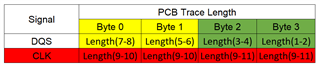
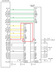
We've designed a new PCB based on DRA77P with 4GB, so we're using two EMIF. With one of the EMIF we've done what is desceribed on Figure 7-55. 32-Bit, One-Bank DDR3 Interface Schematic Using Two 16-Bit DDR3 Devices, page 456 of the short datasheet SPRS993E. This is, DDR1_CK (red line) goes firts to the device that had the LSB (DDR1_D0...DDR1_D15, yellow line) and then to MSB device (DDR1_D16...DDR1_D31, green line).
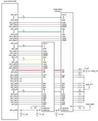
But on the second EMIF, this is different. DDR2_CK goes first to the MSB device (DDR2_D16...DDR2_D31) and then to the LSB (DDR2_D0...DDR2_D15).
When I fullfil the "EMIF Tool: Register Configuration" excel, I have a doubt, regarding EMIF2: what is Byte 0? Are the bytes related to DDR2_D0...DDR2_D15 or to DDR2_D16...DDR2_D31?
Regards,