Other Parts Discussed in Thread: TDA4VH
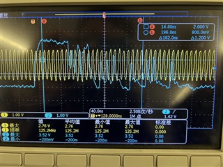
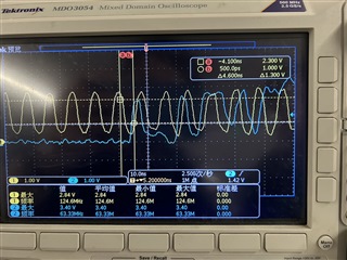
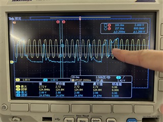
Two TDA4VH chips connect the MAC to MAC through the RGMII interface of the main domain; Gigabit communication debugging failed; The oscilloscope measurement shows that the TX data signal cannot be reached chip's level threshold; As shown in the figure below, data 01 is followed by 11, resulting in the level of 0 being raised. Similarly, 10 is followed by 00, resulting in 1 level being pulled down. I feel that the data-driven ability is too poor; Could you help me if there are registers that can be configured and modified to improve the driving ability of data signals? In addition, why is the clock signal normal for the same length?