Because of the Thanksgiving holiday in the U.S., TI E2E™ design support forum responses may be delayed from November 25 through December 2. Thank you for your patience.

This thread has been locked.

If you have a related question, please click the "Ask a related question" button in the top right corner. The newly created question will be automatically linked to this question.

TDA4VH-Q1: Two TDA4VH chips connect the MAC to MAC through the RGMII interface of the main domain; Gigabit communication debugging failed

Part Number: TDA4VH-Q1
Other Parts Discussed in Thread: TDA4VH

Application:Two TDA4VH chips connect the MAC to MAC through the RGMII interface of the main domain;The PCB trace lengths of the TX / RX / CLK channel are about 8000 mil.

Problem:

  • The 100 Mbit/s communication is normal

  • The 1000 Mbit/s communication is failed

Test:

The oscilloscope measurement shows that the TX data signal cannot be reached chip's level threshold;
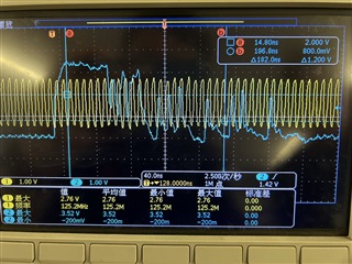
First:

As shown in the figure below, data 01 is followed by 11, resulting in the level of 0 being raised. Similarly, 10 is followed by 00, resulting in 1 level being pulled down.
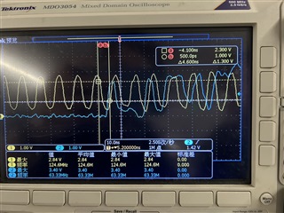
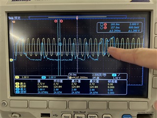
Second:

Through the IBIS simulation model and extracting the S parameters of the PCB board for simulation analysis, the simulation results are not very poor and can meet the high and low threshold of the signal.But the signal measured by high-speed oscilloscope is really poor (The test position of the probe is at the via of the chip at the receiving end, and the GND is very short); At present, it seems that the IBIS simulation model is inconsistent with the actual test.

Then We disconnect the load and measure the TXCLK signal at the chip sending source. It is found that the slope of the rising edge of the clock waveform is very slow; Is this the lack of drive capability of the chip itself?

The above image measurement position is at the source disconnection string resistance,the trace of the 8000mil PCB has been disconnected,the measurement point is about 400 mil away from the chip.

In view of the above phenomena,we have two questions:

1.In our experience,RGMII pin locate at MCASP BANK.Too many multiple functions may produce more capacitive reactance.Is the problem caused by the backflow current between the multiplexed pins?

2.Is there any other method to improve drive capability.

  • To confirm your configuration - the scope image provided of just clock is disconnected from the load/long trace. Connected is approx 400mil of trace and a measurement point is near the end.  Is that correct?  The scope plots showing the data and clock is measured where (near source or receiver)?

    Regarding the drive capability - that information was provided previously in this E2E.

    https://e2e.ti.com/support/processors-group/processors/f/processors-forum/1200155/faq-tda4vm-q1-tda4-drive-strength-controls

    What is the power supply voltage for the VDDSHV power rail?  Is it low (3.15V), causing the IO max voltage to be reduced?  Or does it dip during RGMII usage due to high inductance/insufficient decoupling on the IO power rail?

  • To confirm your configuration - the scope image provided of just clock is disconnected from the load/long trace. Connected is approx 400mil of trace and a measurement point is near the end.  Is that correct?

    Reply:YES

     The scope plots showing the data and clock is measured where (near source or receiver)?

    Reply:The first three pictures near  receiver.The fourth picture near source.

    We test the power is normal,it is always at 3.3V.And we have enough capacitance at the Power Pin.The power is connected directly to the pin which have no high inductance.

  • Can you provided your simulations data?  I would like to see the simulation data matching the clock waveform you are sharing.  My license is not currently working on my simulation program, so unable to replicate myself.

    Note the data transfer scope captures are appear to be NOT captured using a scope with sufficient bandwidth.  The scope used to capture the clock waveform looks like much higher bandwidth - that is the reason I am first focusing on it.  If possible - please re-capture the data transfers using a high bandwidth scope.

  • The simulation results for a data bit was provided via email.  

    1.  It looks like the VIHmin of 0.8V is ‘barely’ reached, yes? Do you have the simulation of the clock captured, since that is what was captured on the scope?[Response]  Yes, it did not reach the 0.8V voltage of VIHmin. The clock waveform has been measured and it can be reached VIHmin voltage of 0.8V.T

    [TI] The clock waveform simulation data was not provided for review.

    2.  These waveforms are generated via what tool – Hyperlynx (or similar 2D tool)? 2D tools do not model the PCB’s 3D elements (vias) very well. They may explain why the actual measurements look little ‘worse’ than the simulated data.

    [Response]  We are using a 2.5D simulation tool. The signal rate is 250Mbps, which is not very high. The difference between 2D simulation software and 3D simulation software should not be too significant. We tested the waveform of a CLK at the chip source, and the subsequent link was disconnected. Compared with the simulated waveform, it is better to see the difference between the output of the IBIS model and the actual measurement.

    [TI] Yes - vias can have impact on simulation results (just like no loss vs lossy simulations did).