This thread has been locked.

If you have a related question, please click the "Ask a related question" button in the top right corner. The newly created question will be automatically linked to this question.

AM6442: GPMC Single Write, Non-Multiplexed

Guru 10255 points

Part Number: AM6442

Tool/software:

Hi Support Team,

I apologize for regarding a thread that has been ongoing for some time,
but I have additional questions regarding the following site.

e2e.ti.com/.../

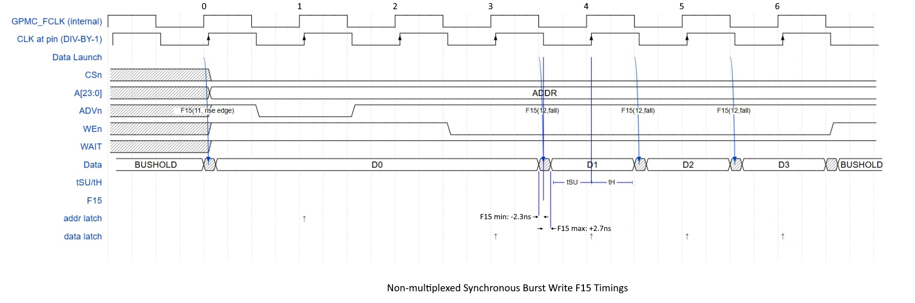
The customer is using Single Write, Non-Multiplexed, so only the first transfer will be performed.

In the case of Single Write, Non-Multiplexed, referring to
Figure 6-43. GPMC and Multiplexed NOR Flash — Synchronous Burst Write
in the datasheet, please let me know what the value of “F15” would be.

Please confirm the appropriate value below.

  To clarify, the question in the image is as follows.  

Q1. F15 is specified for Transition. Here, the minimum is 17.7 ns, but
the maximum is 22.7 ns, so it cannot be captured even in the next clock.
If it is specified for Setup, I think 17.7 ns is reasonable, but is that correct?

Q2. F15 is specified for Transition. Here, if it is specified for Hold,
I think 22.7 ns is reasonable for the maximum, but is that correct?
.

I would also like to confirm the timing diagram and specification values for Single Write and Multiplexed cases.

Best Regards,
Kanae

  • Hi Kanae,

    Please give me 1-2 days to familiarize myself with this and the older thread.

    Thanks,

    Stan

  • Hi Stan,

    Thank you for your support.
    I am waiting for your reply.

    Best Regards,
    Kanae

  • No problem.

    Thanks,

    Stan

  • Hi Stan,

    Thank you for your support.

    Is there any progress on this matter?
    As I need to report to the customer, could you please let me know when you can provide a response?

    Best Regards,
    Kanae

  • Hi Kanae,

      is working on this. Please expect his response by tomorrow.

  • Hi Stan,

    Thank you for your support!
    I expect the response from Anastas Yordanov.

    Best Regards,
    Kanae 

  • Hello Kanae,

    Today I sent an internal query to our GPMC expert with the purpose to clarify some time reference points used in the definition of the F15, F12 and F13 parameters. I consider this as the necessary step before I am able to do a correct timing analysis. So I am awaiting his response (hopefully by tomorrow EOB).

    Meanwhile I have some questions to you:

    Q1. F15 is specified for Transition. Here, the minimum is 17.7 ns, but
    the maximum is 22.7 ns, so it cannot be captured even in the next clock.
    If it is specified for Setup, I think 17.7 ns is reasonable, but is that correct?

    Q2. F15 is specified for Transition. Here, if it is specified for Hold,
    I think 22.7 ns is reasonable for the maximum, but is that correct?

    I am afraid I did my best to understand the customer questions Q1 and Q2 but I failed because I am missing more details in the attached diagram. So several questions from my side:

    A/ "F15 is specified for Transition" ? I guess the customer meant F15 is specified for the "delay time" from valid data output on the data bus until data transition occurs.

    B/ What can not be captured in the next clock in the Q1 case ?

    C/ Why would one want to have F15 matching the F12 (setup time) in Q1 case

    D/ why would one want to have F15 matching the F13 (hold time) in the Q2 case ?

    I am a bit confused between what AM6442 DS represents as F15 timing in the GPMC Synchronous write diagrams ( time from the data latch point until data transition ) and my understanding of F15 from your previous discussions with the GPMC expert. According to your discussions F15 is the entire time (data width) from the moment data is output valid by the GPMC until data transition, and in this case F15 = F12 + F13. But  F12_min (1.81 ns) + F13_min (2.29 ns) <<  F15_min = 17.7 ns.  I am trying to clarify this with the same expert now. 

    D/ Would you mind re-drawing the diagram with more time reference points, details and remarks to help me understand the customer main questions Q1 and Q2.

    For example, specify if Data is Data 0 (Note 11 & 12 applicable) or Data 1...n (Note 12 applicable). Mark the setup and hold time intervals on the diagram, to help me understand why the min 17.7 ns would be ok for setup time in your Q1 case and why the max 22.7 ns would be ok for a hold time in your Q2 case.

    I understand that in the F15 calculation for the Data 1 through the Data n, J = P / 2 = 20 /2 = 10 ns (half cycle time) shall be used and not P = 20ns because of the Notes 12 and 13 to the F15 description. I also understand that J = P / 2 shall be used to calculate the worst case hold time for Data 0 in GPMC synchronous burst write scenarios.

    P/2 - 2.3 = 10 - 2.3 = 7.7 ns

    P/2 + 2.7 = 10 + 2.7 = 12.7 ns

    Thanks for your patience !

    Kind Regards,

    Anastas Yordanov

  • Hi Anastas Yordanov,

    Thank you for your support. 
    I look forward to a response from the GPMC expert. 

    I will also comment on the details you provided.

    Anastas Yordanov said;
    Today I sent an internal query to our GPMC expert with the purpose to clarify some time reference points used in the definition of the F15, F12 and F13 parameters.

     My customer is referring to the data sheet Figure 6-43. GPMC and Multiplexed NOR Flash — Synchronous Burst Write and inquiring about Single Write. I suppose the parameters F12 and F13 related to Read are not necessary.

     Anastas Yordanov said;
    A/ "F15 is specified for Transition" ? I guess the customer meant F15 is specified for the "delay time" from valid data output on the data bus until data transition occurs.

    Yes. As you understand, F15 is specified for the “delay time” from the valid data output on the data bus until the data transition occurs.

     Anastas Yordanov said;
    B/ What can not be captured in the next clock in the Q1 case ?

    My apologies for the insufficient explanation. As noted in the referenced thread, the customer is assuming J = GPMC_CLK at 50MHz, resulting in J=GPMC_CLK=20ns.
    In this case, the minimum value of 17.7ns allows capture on the next clock cycle, but the maximum value of 22.7ns does not allow capture on the next clock cycle, leading to the above question.

     Anastas Yordanov said;
    C/ Why would one want to have F15 matching the F12 (setup time) in Q1 case

    Regarding F12, it is not specifically mentioned here. Please clarify the specified value for Single Write.

    Anastas Yordanov said;
    D/ why would one want to have F15 matching the F13 (hold time) in the Q2 case ?

    Regarding F13, it is not specifically mentioned here. Please clarify the specified value for Single Write.

     Anastas Yordanov said;
    According to your discussions F15 is the entire time (data width) from the moment data is output valid by the GPMC until data transition, and in this case F15 = F12 + F13. But  F12_min (1.81 ns) + F13_min (2.29 ns) <<  F15_min = 17.7 ns.  I am trying to clarify this with the same expert now.

    I suppose it's the difference between Read and Write, but please point out if my understanding is incorrect. As stated above, F12 and F13 are not specifically mentioned here.

     Anastas Yordanov said;
    I understand that in the F15 calculation for the Data 1 through the Data n, J = P / 2 = 20 /2 = 10 ns (half cycle time) shall be used and not P = 20ns because of the Notes 12 and 13 to the F15 description.

    I also understand that Note 12 and 13 specify using J = P / 2 = 20 / 2 = 10ns (half-cycle time) instead of P = 20ns. However, since this is a Single Read, I believe Note (11) “First transfer only for CLK DIV 1 mode.” is applicable, right?

     Anastas Yordanov said;
    I also understand that J = P / 2 shall be used to calculate the worst case hold time for Data 0 in GPMC synchronous burst write scenarios.
    P/2 - 2.3 = 10 - 2.3 = 7.7 ns
    P/2 + 2.7 = 10 + 2.7 = 12.7 ns

    If this case is applicable to F11, is it correct to calculate as follows?

     P - 2.3 = 20 - 2.3 = 17.7 ns
     P + 2.7 = 20 + 2.7 = 22.7 ns

    Best Regards,
    Kanae

  • Hi Kanae,

    I suppose the parameters F12 and F13 related to Read are not necessary.

    You are right, thanks. I also got confirmation from the expert yesterday, that the F12 and F13 are related to GPMC READ transactions and the F15 related to the GPMC Write transactions. 

    Yes. As you understand, F15 is specified for the “delay time” from the valid data output on the data bus until the data transition occurs.

    I am not sure in the correctness of my understanding from your previous discussion: F15 delay time starts at the moment when GPMC outputs valid data (on clock rising edge D0 or clock falling edge for D1..n).

    Here is why:

    According to such a F15 definition,  F15 min = P - 2.3 = 20 - 2.3 = 17.7 ns will not allow the external memory to latch the data on the next GPMC_CLK rising edge because the valid data time width (according this definition of F15) is lower than the period P. In this case a non-valid data during transition is captured. 

    In the F15 = P nominal case the time interval for latching a valid data will be very tight (not practical).

    For  F15 max = P + 2.7, a valid data can be latched. 

    F15 shall have a different definition and I have to crosscheck it with the expert.  

    I am still awaiting answers from the expert to my questions on key clock time reference points. 

    I will add your questions, as follows:

    Q1. What is the definition of the F15 parameter (with a detailed representation on a timing diagram with the GPMC_FCLK, GPMC_CLK, WEn and A/D signals) 

    Q2. How is the setup time tsu defined for a GPMC Synchronous Single Write transaction ? (There is no such formulae in the DS)

    Q3. How is the hold time th defined for a GPMC Synchronous Single Write transaction ? (There is no such formulae in the DS)

    However, since this is a Single Read, I believe Note (11) “First transfer only for CLK DIV 1 mode.” is applicable, right?

    Q4. I think you meant GPMC Synchronous Single Write. Correct ? 

    If this case is applicable to F11, is it correct to calculate as follows?

     P - 2.3 = 20 - 2.3 = 17.7 ns
     P + 2.7 = 20 + 2.7 = 22.7 ns

    Q5. I suppose you meant calculation of the F15 MIN and F15 MAX values according Note 11 for the GPMC Synchronous Single Write case. Ok ?

    Thanks

    Regards,

    Anastas Yordanov

  • Hi Anastas Yordanov,

    Thank you for your reply!

    So you are currently asking the GPMC expert about Q1-Q3, correct?
    Since I need to report back to the customer, could you please let me know
    when you expect to receive their response?

    Regarding Q4 and Q5, your understanding is correct.

    Additionally, I seem to have a different understanding of F15 based on the diagram you provided above.
    Since the datasheet does not mention Single Write, Non-Multiplexed , therefore referring to
    Figure 6-43. GPMC and Multiplexed NOR Flash — Synchronous Burst Write,
    I would simply like to confirm the maximum and minimum values for the red area below.

    As I posted in my first post, I would also like to confirm the timing diagram
    and specification values for
     Single Write, Multiplexed cases.

    Best Regards,
    Kanae

  • Hello Kanae,

    I've sent your new questions to the GPMC expert with reminder for answers to your previous questions (Q1-Q3) and the others. 

    I requested from him expected time for answers to customer Q1-Q3 and the other questions.

    I expect to get a response from him by tomorrow. 

    Thanks for your patience !

    Kind Regards,

    Anastas Yordanov

  • Hi Anastas Yordanov.

    Thank you for your support.

    Even if responses from the GPMC expert are not yet complete,
    it is necessary to report at least the estimated timeline for
    a response to my customer.
    I appreciate your continued cooperation.

    Best Regards,
    Kanae

  • Hi Kanae,

    Anastas is out of office today and on Monday. I'm copy/pasting the initial response from Mark without modification:

    "

    Customer has read the datasheet F15 timing and understood delay from GPMC_CLK rising edge to data becoming valid on the bus is between (one GPMC_FCLK cycle - 2.3ns) and (one GPMC_FCLK cycle + 2.7ns). For their GPMC_FCLK period of 20ns the datasheet tells that the data will transition on the bus between 17.7ns and 22.7ns after the rise edge of GPMC_CLK that initiates the data launch onto the bus.

    Points to clarify:

    • GPMC_FCLK is the internal clock that runs the state machine - it cannot be measured and no datasheet timing can reference this clock edge.
    • GPMC_CLK is the external clock that can be measured - in divide-by-one mode, it is the GPMC_FCLK delayed by internal logic and the IO buffer delay. Delays through the IO buffers can vary, so it is possible that signals may arrive at the pins earlier than GPMC_CLK - so there can be a negative delay from GPMC_CLK to a signal like Data valid on the bus.

    I believe there is a miscommunication by the datasheet. The data will more likely become valid on the data bus between -2.3ns and +2.7ns from the GPMC_CLK edge aligned with the GPMC_FCLK internal clock edge that launches data onto the bus.

    For non-multiplexed mode, the first data launches onto the bus at the very beginning of the GPMC write cycle (regardless of CLK activation time or CLK divider). If CLK activation is 0 then the CLK rise edge also occurs at the very beginning of the GPMC write cycle. The data may appear up to 2.3ns before the rise edge of GPMC_CLK or up to 2.7ns after the rise edge of GPMC_CLK.

    For multiplexed mode, the parameter WRDATAONADMUXBUS picks which GPMC_FCLK cycle the data bus transitions from address to data. The data may appear up to 2.3ns before the rise edge of GPMC_CLK that corresponds to the GPMC_FCLK rise edge defined by WRDATAONADMUXBUS or up to 2.7ns after the rise edge of GPMC_CLK that corresponds to the GPMC_FCLK rise edge defined by WRDATAONADMUXBUS.


    I think the datasheet min max columns for F15 including J is a mistake (J = GPMC_FCLK per note 10)


    Additionally, the datasheet figures are incomplete because they do not provide details about GPMCFCLKDIVIDER.

    If GPMCFCLKDIVIDER is 0 (div-by-1) then all data launched after initial data is launched on falling edge of GPMC_FCLK which is in phase with GPMC_CLK (half cycle timings). First data is launched at beginning of the write cycle (non-multiplexed) or first data is launched at WRDATAONADMUXBUS time for AD-multiplexed mode.


    If GPMCFCLKDIVIDER is greater than 0 (div-by-2,-3, or -4), then all data launches on rising edge of GPMC_FCLK, which can correspond to a falling edge of the divided GPMC_CLK. It is not enforced by the IP however, and the register configuration must align GPMC_CLK appropriately so that data launches on the expected edge. The GPMC_CLK can be aligned by using CLKACTIVATIONTIME to delay first rising edge of GPMC_CLK after the beginning of the GPMC write cycle.


    WRACCESSTIME determines when the burst transitions from first data to subsequent data.


    It would provide clarity to measure with an oscilloscope the delay from CLK edge to data valid after...

    • WRDATAONADMUXBUS
    • WRACCESSTIME

                   Like I did with E2E where I confirmed initial data appears on the bus at the start of write cycle regardless of CLK divider and CLKACTIVATIONTIME (https://e2e.ti.com/support/processors-group/processors---internal/f/processors---internal-forum/1533122/am3352-gpmc-the-signal-timing)

                   I suspect the Data will depend only on GPMC_FCLK - and there is no dependency of GPMC_CLK

    "

  • Hi Stan,

    Thank you for your reply.

    I understand you provided Mark's preliminary response.
    I am sure that you will provide detailed answers later,
    but at this point, I would like to confirm the following points regarding these answers.

    Mark said;

    I believe there is a miscommunication by the datasheet. The data will more likely become valid on the data bus between -2.3ns and +2.7ns from the GPMC_CLK edge aligned with the GPMC_FCLK internal clock edge that launches data onto the bus.

     Mark said;

    I think the datasheet min max columns for F15 including J is a mistake (J = GPMC_FCLK per note 10)
    Additionally, the datasheet figures are incomplete because they do not provide details about GPMCFCLKDIVIDER.

    Q1. When do you plan to correct the inaccuracies in the above datasheet?

    Q2. Could you please provide a timing chart for Single Write, Non-Multiplexed and Single Write, Multiplexed that reflects the correct parameters?

    Mark said;

    This indicates that, as I verified end-to-end, the initial data appears on the bus at the start of the write cycle,
    regardless of CLK division or CLKACTIVATIONTIME.
    (Reference: e2e.ti.com/.../am3352-gpmc-the-signal-timing)

    Q3. The link above displays an error and cannot be verified.
          Could you please make the content publicly available?

    Best Regards,
    Kanae


  • Hi Kanae,

    I and Anastas we are on bank holidays in our country. We are online tomorrow. For Q3 I'm pasting the last response from the internal thread:

    "I checked signal waveforms on the oscilloscope to confirm the below findings...
    As I suspected in non-AD-multiplexed mode, the first data is always on bus at the start of the cycle.
    The first data will be on the bus at the start of the cycle regardless of CLK activation time or CLK divider settings.
    Depending on the CLK activation setting, the data can appear on the bus before the CLK starts. The datasheet makes it seem like the data will launch only at first rising CLK edge for div-by-1 or only on first falling edge for div-by-2/3/4... but I have observed that the first data is always launched on the bus at the start of the cycle.

    Regarding the second data of a burst... In div-by-1 mode the 2nd data (and subsequent data) always launches on falling CLK edge.
    However, in div-by-2/3/4 it is possible for 2nd data (and subsequent data) to launch on rising or falling CLK edge. The configuration of GPMC needs to be set correctly to ensure data is valid for whichever CLK edge is used to latch data (typically rising edge).


        Test 1 div-by-1, CLK ACT 0, PAGEBURSTACCESSTIME = 1
            First data on bus at cycle start at CLK rise edge
            2nd data launch on falling CLK edge
            
        Test 2 div-by-1, CLK ACT 1, PAGEBURSTACCESSTIME = 1  
            First data on bus at cycle start, 1 FCLK cycle before first CLK rise edge
            2nd data launch on falling CLK edge
        
        Test 3 div by 2, CLK ACT 0, PAGEBURSTACCESSTIME = 1
            First data on bus at cycle start, at first rise edge of CLK
            2nd data launch on rising CLK edge... this is a problem for timing closure since valid data cannot be latched - launches on rise CLK edge, "transitions to invalid" on falling CLK edge - there is no CLK edge to latch data - PAGEBURSTACCESSTIME must be set to 2 with CLK div-by-2 (see Test 5 and Test 6)
            
        Test 4 div by 2, CLK ACT 1, PAGEBURSTACCESSTIME = 1
            First data on bus at cycle start, 1 FCLK cycle before first CLK rise edge
            2nd data launches on falling CLK edge - but also "transitions to invalid" on following rise edge - need to set PAGEBURSTACCESSTIME must be set to 2 with CLK div-by-2 (see Test 5 and Test 6)
            
        Test 5 div by 2, CLK ACT 0, PAGEBURSTACCESSTIME = 2
            First data on bus at cycle start, at rising edge of CLK
            2nd data launches on rising CLK edge - "transitions to invalid" on following rise edge (could be latched on neg edge, but this is not normal)

        Test 6 div by 2, CLK ACT 1, PAGEBURSTACCESSTIME = 2
            First data on bus at cycle start, 1 FCLK cycle before first CLK rise edge
            2nd data launches on neg CLK edge - "transitions to invalid" on following neg edge (could be latched on rise edge as recommended)

    "

  • Hi Stan,

    Thank you for your support.
    I will share the Q3's website contents with my customer.

    Regarding the following points you provided previously, my customer commented:
    “It's a bit disappointing that it's phrased as ‘The data will more likely become valid on...’
    rather than providing guaranteed values, especially since we're asking the manufacturer.”

    Mark stated:
    I believe there is a miscommunication by the datasheet.
    The data will more likely become valid on the data bus between -2.3ns and +2.7ns from the GPMC_CLK edge aligned with the GPMC_FCLK internal clock edge that launches data onto the bus.

    Could you please let us know when you expect to post the responses for Q1 and Q2?

    Best Regards,
    Kanae

  • Hello Kanae,

    Q1. When do you plan to correct the inaccuracies in the above datasheet?

    Q2. Could you please provide a timing chart for Single Write, Non-Multiplexed and Single Write, Multiplexed that reflects the correct parameters?

    I am waiting the experts to let us know the expected time for answering  Q1 and Q2.

    I hope to get their confirmation today or tomorrow.

    Kind Regards,

    Anastas Yordanov

  • Hi Anastas Yordanov,

    Thank you for your reply.
    I would appreciate following up on the expert's answers.

    Best Regards,
    Kanae

  • Hello Kanae,

    I've sent a reminder but our GPMC expert might be a bit more busy than usual these days.

    I would appreciate following up on the expert's answers.

    Which of the already received answers from the expert need clarification from my side ?

    I appreciate your patience !

    Thanks

    Kind Regards,

    Anastas

  • Hi Anastas,

    Thank you for your support.

    I would like to know the answers to Q1 and Q2 that I have already requested as soon as possible. 

    If it is difficult to handle, please check with your expert for a schedule for the answer at least
    so that I need to report to my customer.

    Best Regards,
    Kanae

  • Hello Kanae,

    The GPMC expert is currently working on the requested time charts (Q2) and will provide them early next week.

    Regarding Q1 - I sent a reminder to the DS documentation team. I also expect to get the answer early next week.

    Thanks

    Kind Regards,

    Anastas Yordanov


  • Hi Anastas,

    Thank you for your support.

    I will share it with my customer.

    Best Regards,
    Kanae

  • Hi Kanae,

    Thanks. I will provide them once available.

    Best Regards,

    Anastas

  • Responding to Q2... please refer to below timing diagrams.

    Timings are from GPMC_CLK crossing mid-supply voltage (VDD/2) to DATA bus crossing mid-supply voltage (VDD/2).
    If you need to compare against VIH/VIL crossing, then it is recommended to perform IBIS simulation of the IO buffer, PCB, and endpoint (memory/FPGA) IBIS model to learn the rise/fall slew rates from mid-supply voltage (VDD/2) to VIH/VIL.
    F15 defines the min/max delay from the specified GPMC_CLK edge (at the pin) to the data valid (at the pins). Between F15 min and max timing, the data is invalid. Data valid means that the data has crossed VDD/2.

  • Hi Mark,

    Thank you for your support!
    I will share the response to Q2 with my customer.

    Regarding Q1, when can I receive the response?
    Please provide the current schedule for updating the datasheet.

    Best Regards,
    Kanae