Dear Ti Support,
life is not perfect and I have to implement a new board using TMS320C6424.
I have spend quite a time digging into manuals. Though there were several errors and inconsistency in the docs I almost solved my issue.
So far I fail to boot this device from NAND Flash. NAND is connected on CS2, FPGA connected on CS3. I use FPGA (Signal Tap) to monitor status of the NAND bus. Following works:
1. NAND programming/reading using SoC's ECC calculation and check
2. NAND read by TMS320C6424 boot rom
I can see that my AIS is read properly at SIgnal Tap. So I am confident that Flash get recognized by the boot rom, proper page and block sizes are used. But nothing happens and boot rom keeps reading next.
It guess that either my AIS is incorrect or page read fails ECC check. Both are not documented completely.
1. What NAND's spare area layout should I use? I found a few examples for old DM6x DSPs and implemented in same way. No clue whether it is correct.
2. NAND's AIS there are 3 fields after Magic Number, that are not completely documented:
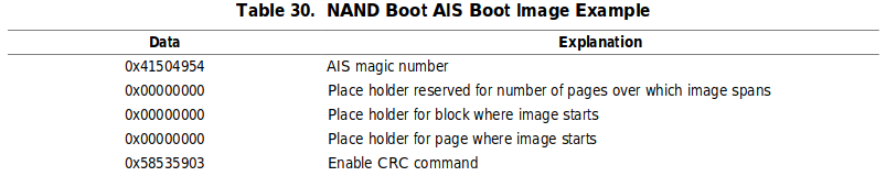
I checked genAIS.pl script without luck. I have a block size of 0x40 pages. If my sample AIS fits into single page and is programmed into 1-st block, than I should use here 0x1, 0x1, 0x0? Or maybe 0x1, 0x1, 0x40?
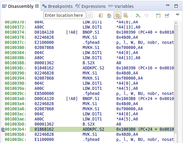
Anyway, since ROM code can be debugged I end up digging into disassembly. Looks like code is compiled without optimization. Though it is going to be quite time consuming I guess I can solve my issues by debugging ROM code.
I guess you are not going to update C6424 documentation, so maybe you can share source code for the boot rom? It could save my time. We plan to do PCI boot also and I suspect I am going to face more issues with this DPS.