This thread has been locked.

If you have a related question, please click the "Ask a related question" button in the top right corner. The newly created question will be automatically linked to this question.

TMS320C6414T: SPI slave delay parameter DX valid

Part Number: TMS320C6414T

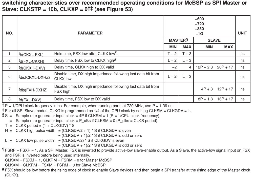
For SPI port as a slave, in any mode, the data sheet defines the Dx valid delay from Clock parameter as:

12P + 2.8 min, and 20P + 17 max, where P is the period of the internal DSP clock.

For Dx valid delay parameter definition, are the constant terms (2.8, 17) dependent on temperature and die variations only? If not what are the dependencies?

For Dx valid delay  parameter definition, are the "P" terms (12P , 20P), is the variation (12 - 20) a function of internal DSP timing with the SPI port only? is this variation seen for all SPI configurations? Or is it tighter in some configurations? Can this "P" term be characterized for SPI configuration, DSP configuration and/or temperature environment?

  • Hello Eric,

    This timing defines when the Dx (MOSI from DSP slave to master) becomes valid after external clock edge is input to the DSP.

    In slave mode, it takes multiple SYSCLK cycles to detect the change in the incoming CLK signal (12 to 20 CPU clock cycles, P). P = 1/CPU clock frequency in ns. For example, when running parts at 720 MHz, use P = 1.39 ns

    The 2.8ns to 17ns output delay is the additional "analog" delay for the signal to propagate from the SPI module to the pin. It will have been timing closed across process, voltage, and temperature - either guaranteed by design or tester characterized at the worst case PVT corner.

    All silicon received from TI will perform within these timing specifications. I cannot tell you which PVT corner is responsible for the worst case numbers unfortunately.

    You might be able to reproduce similar numbers by adjusting the voltage and temperature on the silicon you have. You cannot, however, request slow, fast, or typical silicon from TI to find the worst case PVT corner. You will not be able to identify if the silicon you have is slow, fast, or typical either.

    It will likely perform somewhere in the middle of these timing specifications.

    Does this help?

    Regards,
    Mark

  • Mark,

    Yes this helps a lot - and thank you for your quick response.

    Have we seen such large variation of 2.8 - 17ns, (14ns) in other output pure prop delays in this IC?  And if not, then  why with this I/O pin? A 14ns variation for PVT seems very high to me.  I would suspect other pins in the same die and environment would reflect similar delays also.

    Is a portion of this delay  configuration dependent in how this port is muxed to the I/O pin? Although the datasheet specs this delay the same for all modes, is it dependent on the MODE (CLKSTP, CLKXP)?  Or is the variation dependent on which of the SPI port (3) is in use?

    And if so can we characterize further?  Could you please investigate.

    Thanks Again

  • Hi Eric

    This is very old device and recently also NRND. 

    We will not be able to support any additional characterization/ investigation for this device and the data in its datasheet. The effort for such an investigation is non trivial.

    Regret if this causes issues for you, but I  wanted to make sure the support expectation is understood on this device family. 

    Regards

    Mukul 

  • Mukul,

    Thanks for investigating. You can close this post out.