This thread has been locked.

If you have a related question, please click the "Ask a related question" button in the top right corner. The newly created question will be automatically linked to this question.

TMDSLCDK138: TMDSLCDK138 boot failed

Part Number: TMDSLCDK138
Other Parts Discussed in Thread: OMAPL138

Hi,

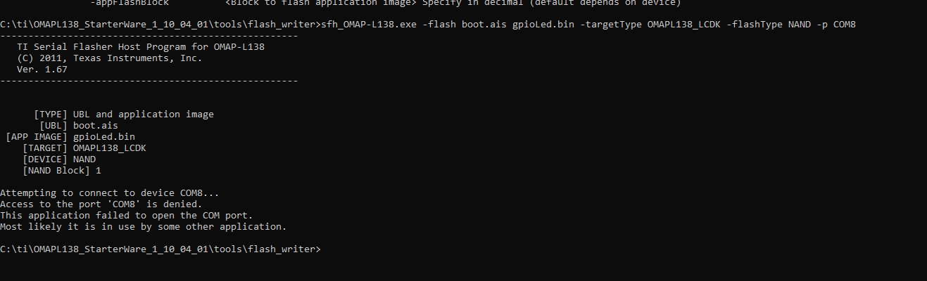
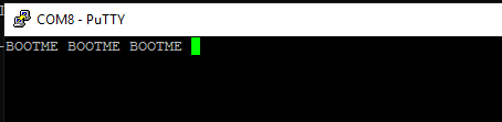
I have bought TMDSLCDK138. I want to boot from nand flash. I have burned a simple gpio demo successfully and i have set boot mode to nand flash (sw1 2/3/4 on 1 off). But the gpio didn't work when i powered on again.

 I load cfg file from aisgen\AISgen for D800K008\cfg_files\C6748_LCDK_AISGen_Config.cfg to aisgentool.

core clk:300M/DDR:150M which are the same to my GEL configuration.

How to solve my problem?

  • Hi,

    Which Processor SDK is this?

    Best Regards,
    Yordan

  • Hello,

    Please take a look at the following application notes. If you still have any questions please let us know.

    Using the OMAP-L132/L138 Bootloader

    OMAPL138/C6748 ROM Bootloader Resources and FAQ

    Regards,
    Sahin

  • Hi,

    Yes,i have read links you posted above. And I tried to use ccs

    to track my program. But I don’t know how to debug. Which is key point I should concentrate on when debug. Because i am not familiar with assembly.I will attach picture later.

  • Hello, 

    Since you have the LCDK138, please use "OMAPL138_LCDK_AISGen_Config.cfg"

    If that does not work, please run this debug GEL file (after your board has booted from nand) and post its output here.

    8662.OMAPL1x_debug_v9_CCSv6.zip

    Regards,
    Sahin

  • Hi,

    I have changed to OMAPL138_LCDK_AISGen_Config.cfg. But it still failed.

    This is output log of debug GEL:

    ---------------------------------------------
    C674X_0: GEL Output: | Device Information |
    C674X_0: GEL Output: ---------------------------------------------
    C674X_0: GEL Output: DEV_INFO_00 = 0x1B7D102F
    C674X_0: GEL Output: DEV_INFO_01 = 0x00000000
    C674X_0: GEL Output: DEV_INFO_02 = 0x00000010
    C674X_0: GEL Output: DEV_INFO_03 = 0x00000035
    C674X_0: GEL Output: DEV_INFO_04 = 0x00000000
    C674X_0: GEL Output: DEV_INFO_05 = 0x000003E0
    C674X_0: GEL Output: DEV_INFO_06 = 0x00000080
    C674X_0: GEL Output: DEV_INFO_07-DEV_INFO_08-DEV_INFO_09-DEV_INFO_10-DEV_INFO_11-DEV_INFO_12 = 0-0-5634736-13-14-35
    C674X_0: GEL Output: DEV_INFO_13,DEV_INFO_14,DEV_INFO_15,DEV_INFO_16 = 5,0,0,11237
    C674X_0: GEL Output: -----
    C674X_0: GEL Output: DEV_INFO_17 = 0x00030003
    C674X_0: GEL Output: DEV_INFO_18 = 0x00000000
    C674X_0: GEL Output: DEV_INFO_19 =C674X_0: GEL Output: 0C674X_0: GEL Output: 0C674X_0: GEL Output: 0C674X_0: GEL Output: 0C674X_0: GEL Output: 0C674X_0: GEL Output:
    C674X_0: GEL Output: -----
    C674X_0: GEL Output: DEV_INFO_20 = 0x30303864
    C674X_0: GEL Output: DEV_INFO_21 = 0x3830306B
    C674X_0: GEL Output: DEV_INFO_22 = 0x00000000
    C674X_0: GEL Output: DEV_INFO_23 = 0x00000000
    C674X_0: GEL Output: -----
    C674X_0: GEL Output: DEV_INFO_24 = 0x0D02300E
    C674X_0: GEL Output: DEV_INFO_25 = 0x0055FAB0
    C674X_0: GEL Output: DEV_INFO_06 = 0x00000080
    C674X_0: GEL Output: DEV_INFO_26 = 0x57CA0005
    C674X_0: GEL Output:

    C674X_0: GEL Output: ---------------------------------------------
    C674X_0: GEL Output: | BOOTROM Info |
    C674X_0: GEL Output: ---------------------------------------------
    C674X_0: GEL Output: ROM ID: d800k008
    C674X_0: GEL Output: Silicon Revision 2.1
    C674X_0: GEL Output: Boot pins: 16
    C674X_0: GEL Output: Boot Mode: NAND 16
    C674X_0: GEL Output:
    ROM Status Code: 0x00000001
    Description:C674X_0: GEL Output: DSP was put to sleep
    C674X_0: GEL Output:
    Program Counter (PC) = 0x00700000
    C674X_0: GEL Output:
    C674X_0: GEL Output: ---------------------------------------------
    C674X_0: GEL Output: | Clock Information |
    C674X_0: GEL Output: ---------------------------------------------
    C674X_0: GEL Output:
    C674X_0: GEL Output: PLLs configured to utilize crystal.
    C674X_0: GEL Output: ASYNC3 = PLL0_SYSCLK2
    C674X_0: GEL Output:
    C674X_0: GEL Output: NOTE: All clock frequencies in following PLL sections are based
    C674X_0: GEL Output: off OSCIN = 24 MHz. If that value does not match your hardware
    C674X_0: GEL Output: you should change the #define in the top of the gel file, save it,
    C674X_0: GEL Output: and then reload.
    C674X_0: GEL Output:
    C674X_0: GEL Output: ---------------------------------------------
    C674X_0: GEL Output: | PLL0 Information |
    C674X_0: GEL Output: ---------------------------------------------
    C674X_0: GEL Output:
    C674X_0: GEL Output: PLL0_SYSCLK1 = 24 MHz
    C674X_0: GEL Output: PLL0_SYSCLK2 = 12 MHz
    C674X_0: GEL Output: PLL0_SYSCLK3 = 8 MHz
    C674X_0: GEL Output: PLL0_SYSCLK4 = 6 MHz
    C674X_0: GEL Output: PLL0_SYSCLK5 = 8 MHz
    C674X_0: GEL Output: PLL0_SYSCLK6 = 24 MHz
    C674X_0: GEL Output: PLL0_SYSCLK7 = 4 MHz
    C674X_0: GEL Output:
    C674X_0: GEL Output: ---------------------------------------------
    C674X_0: GEL Output: | PLL1 Information |
    C674X_0: GEL Output: ---------------------------------------------
    C674X_0: GEL Output:
    C674X_0: GEL Output: PLL1_SYSCLK1 = 24 MHz
    C674X_0: GEL Output: PLL1_SYSCLK2 = 24 MHz
    C674X_0: GEL Output: PLL1_SYSCLK3 = 24 MHz
    C674X_0: GEL Output:
    C674X_0: GEL Output: ---------------------------------------------
    C674X_0: GEL Output: | PSC0 Information |
    C674X_0: GEL Output: ---------------------------------------------
    C674X_0: GEL Output:
    C674X_0: GEL Output: State Decoder:
    C674X_0: GEL Output: 0 = SwRstDisable (reset asserted, clock off)
    C674X_0: GEL Output: 1 = SyncReset (reset assered, clock on)
    C674X_0: GEL Output: 2 = Disable (reset de-asserted, clock off)
    C674X_0: GEL Output: 3 = Enable (reset de-asserted, clock on)
    C674X_0: GEL Output: >3 = Transition in progress
    C674X_0: GEL Output:
    C674X_0: GEL Output: Module 0: EDMA3CC (0) STATE = 0
    C674X_0: GEL Output: Module 1: EDMA3 TC0 STATE = 0
    C674X_0: GEL Output: Module 2: EDMA3 TC1 STATE = 0
    C674X_0: GEL Output: Module 3: EMIFA (BR7) STATE = 0
    C674X_0: GEL Output: Module 4: SPI 0 STATE = 0
    C674X_0: GEL Output: Module 5: MMC/SD 0 STATE = 0
    C674X_0: GEL Output: Module 6: AINTC STATE = 3
    C674X_0: GEL Output: Module 7: ARM RAM/ROM STATE = 3
    C674X_0: GEL Output: Module 9: UART 0 STATE = 0
    C674X_0: GEL Output: Module 10: SCR 0 (BR0/1/2/8) STATE = 3
    C674X_0: GEL Output: Module 11: SCR 1 (BR4) STATE = 3
    C674X_0: GEL Output: Module 12: SCR 2 (BR3/5/6) STATE = 3
    C674X_0: GEL Output: Module 13: PRUSS STATE = 0
    C674X_0: GEL Output: Module 14: ARM STATE = 0
    C674X_0: GEL Output: Module 15: DSP STATE = 3
    C674X_0: GEL Output:
    C674X_0: GEL Output: ---------------------------------------------
    C674X_0: GEL Output: | PSC1 Information |
    C674X_0: GEL Output: ---------------------------------------------
    C674X_0: GEL Output:
    C674X_0: GEL Output: State Decoder:
    C674X_0: GEL Output: 0 = SwRstDisable (reset asserted, clock off)
    C674X_0: GEL Output: 1 = SyncReset (reset assered, clock on)
    C674X_0: GEL Output: 2 = Disable (reset de-asserted, clock off)
    C674X_0: GEL Output: 3 = Enable (reset de-asserted, clock on)
    C674X_0: GEL Output: >3 = Transition in progress
    C674X_0: GEL Output:
    C674X_0: GEL Output: Module 0: EDMA3CC (1) STATE = 0
    C674X_0: GEL Output: Module 1: USB0 (2.0) STATE = 0
    C674X_0: GEL Output: Module 2: USB1 (1.1) STATE = 0
    C674X_0: GEL Output: Module 3: GPIO STATE = 0
    C674X_0: GEL Output: Module 4: UHPI STATE = 0
    C674X_0: GEL Output: Module 5: EMAC STATE = 0
    C674X_0: GEL Output: Module 6: DDR2 and SCR F3 STATE = 0
    C674X_0: GEL Output: Module 7: MCASP0 + FIFO STATE = 0
    C674X_0: GEL Output: Module 8: SATA STATE = 0
    C674X_0: GEL Output: Module 9: VPIF STATE = 0
    C674X_0: GEL Output: Module 10: SPI 1 STATE = 0
    C674X_0: GEL Output: Module 11: I2C 1 STATE = 0
    C674X_0: GEL Output: Module 12: UART 1 STATE = 0
    C674X_0: GEL Output: Module 13: UART 2 STATE = 0
    C674X_0: GEL Output: Module 14: MCBSP0 + FIFO STATE = 0
    C674X_0: GEL Output: Module 15: MCBSP1 + FIFO STATE = 0
    C674X_0: GEL Output: Module 16: LCDC STATE = 0
    C674X_0: GEL Output: Module 17: eHRPWM (all) STATE = 0
    C674X_0: GEL Output: Module 18: MMC/SD 1 STATE = 0
    C674X_0: GEL Output: Module 19: UPP STATE = 0
    C674X_0: GEL Output: Module 20: eCAP (all) STATE = 0
    C674X_0: GEL Output: Module 21: EDMA3 TC2 STATE = 0
    C674X_0: GEL Output: Module 24: SCR-F0 Br-F0 STATE = 3
    C674X_0: GEL Output: Module 25: SCR-F1 Br-F1 STATE = 3
    C674X_0: GEL Output: Module 26: SCR-F2 Br-F2 STATE = 3
    C674X_0: GEL Output: Module 27: SCR-F6 Br-F3 STATE = 3
    C674X_0: GEL Output: Module 28: SCR-F7 Br-F4 STATE = 3
    C674X_0: GEL Output: Module 29: SCR-F8 Br-F5 STATE = 3
    C674X_0: GEL Output: Module 30: Br-F7 (DDR Contr) STATE = 3
    C674X_0: GEL Output: Module 31: L3 RAM, SCR-F4, Br-F6 STATE = 3

  • Hello,

    Please make sure you have followed the steps here: 

    http://processors.wiki.ti.com/index.php/OMAPL138_StarterWare_Booting_And_Flashing#How_to_flash_and_boot_the_sample_DSP_starterware_app_on_OMAPL138_LCDK_board

    You can replace the rasterdisplay example with the gpio example.

    If your project is a SYS/BIOS project, please make sure to follow the guidance in Appendix A of OMAPL138/C6748 ROM Bootloader Resources and FAQ

    Regards,
    Sahin

  • Why COM8 is denied?

  • Hi,

    It works now!

  • That's great to hear!

    Please mark this thread as "Resolved" and I will close it out.

    If you have any other questions let me know.

    Regards,
    Sahin