This thread has been locked.

If you have a related question, please click the "Ask a related question" button in the top right corner. The newly created question will be automatically linked to this question.

AMIC120: ADC malfunction question

Part Number: AMIC120

Hi, 

Customers experienced ADC issues while using AMIC120.

AMIC120 continued to be produced.

However, the 5 newly built boards have problems with ADC operation.

The existing S/W has not been changed.

Customer measured resistance value of pin after AMIC120 was disconnected.

1. Low resistance between ADC1_AIN6(AE16) pin and ADC1_AIN7(AD16) pin.

2. When measuring the resistance between the ADC1_AIN5(Y15) pin and the ADC1_AIN6(AE16) pin, the resistance is measured in open state. (more than 5MΩ)

3. The resistance value between ADC1_AIN6(AE16) pin and ADC1_AIN7(AD16) pin is measured as low as approximately 12k.

Q1. If the resistance value is not normal, what is the problem?

Q2. Please check if there is a possibility that the low measurement is a faulty component.

Top marking

  • Can you provide more details related to the ADC issues they were having before measuring impedance between the ADC input pins?

    I do not recommend measuring the resistance between pins on a semiconductor device before understanding the potential effect of making the measurement.

    The ADC inputs are not fail-safe and should never have any potential applied while the device is not powered. I assume they measured the impedance using a multimeter which applies a potential and measures current to determine the resistance of the load. If so, there is a very good chance this violated the Absolute Maximum Ratings parameter "Steady state max voltage at all I/O pins", which defines a maximum voltage of -0.5V to (IO supply + 0.3V) that can be applied to a pin. In this case, the maximum voltage allowed would be -0.5V - 0.3V when VDD = 0V. There is a very good chance the multimeter open-circuit voltage is greater than 0.3V or -0.5V so they effectively created an Electrical Over-Stress (EOS) condition by making the resistance measurement. I have seen some multimeters that have an open-circuit voltage greater than 7V.

    We need to evaluate their ADC issue based on results when operated within the limits defined by the datasheet.

    Regards,
    Paul

  • Hi Paul,

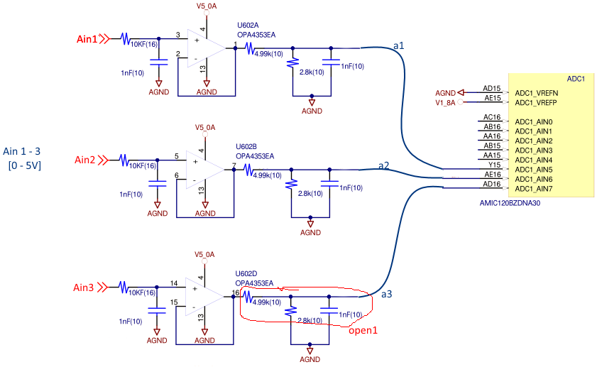
    This is a description of the ADC schematic & test problem.

    ADC schematic

    - There is a 10% difference between a1 point voltage and a2 and a3 point voltage on the same voltage waveform in the schematic.

    As I checked, 2.8k resistance in a1 circuit was measured at 2.4k, while 2.8k resistance in a2 and a3 circuit was measured at 2.0k to 2.1k.

    When all resistance of the line was removed and resistance of a2 point and a3 point was measured to be around 10k to 12k, which is physically equivalent to the resistance between AE16-AD16 pins.

    The resistance between the Y15-AD16 pins & AE16-Y15 pins is measured in M£ units. (measured via an LCR meter)

    In addition, if you remove all elements of the open1 area of a3 circuit, the a2 voltage is output similar to the a1 voltage.

    In addition, when the ADC value is checked, the conversion values of ADC1_AIN6 and ADC1_AIN7 are almost identical when all elements of open1 area of a3 circuit are removed.

    The problem is that the scale is lowered when AIN6-AIN7 of ADC1 is used together.

    (Resistance was not measured with a multimeter / based on ADC conversion value)

    If it is "Electrical Over-Stress (EOS)" condition, please also check why it does not appear between Y15-AD16 pins and AE16-Y15 pins, but only between AE16-AD16 pins.

  • Now I understand what is happening. The source impedance connected to each input is too high relative to the internal resistance between adjacent inputs and this is allowing the potential of one input to affect the adjacent input. You need to look at Figure 12-4. Input Bias Resistors, Bias Supply, and Preamplifier Schematic found in the AMIC120 TRM.

    The following paragraph from the TRM explains the effect of internal coupling between inputs when connected to high impedance sources.

    If the preamplifiers are bypassed, the user may configure a step to use any 1 of the 8 inputs when operating in single-ended mode or any 2 of the 8 inputs when operating in differential mode. However, the effect of the bias resistors and bias supply on the attached voltage source(s) should be considered when using ADC1 as a general purpose ADC. Each internal bias supply has a high output impedance when turned off which will be the case when bypassing the preamplifiers. In this use case, the majority of the input leakage current from any of the analog inputs will be based on the external voltage source connected to the other input associated with the preamplifier. For example, the ADC would measure 0.975 volts on ADC1_AIN1 if it were connected to a 1.0 volt, 1 kohm source while ADC1_AIN2 is connected to a 0.5 volt, 1 kohm source. The error caused by the internal bias resistors can be minimized by connecting the analog inputs to low impedance voltage sources or leaving the other input associated with the preamplifier open-circuit.

    I understand you are using the resistor divider to reduce the 5V output from each op-amp to 1.8V, but this approach will not work with ADC1.

    I'm also concerned the op-amps may be sourcing a potential to ADC pins before it is powered. This would occur if the 5V op-amp power source ramps before the 1.8V VDDA_ADC1 power source. If this happens you are violating the Absolute Maximum Ratings parameter mentioned in my previous reply. The potential applied to the ADC inputs should not exceed -0.5V to 0.3V when the ADC is not powered.

    Using a multimeter or LCR meter to measure resistance of semiconductor pins may create EOS conditions if the output potential of the instrument exceeds the limits defined in the datasheet. It is very unlikely the LCR meter applied a potential less than 0.3V to make the resistance measurement. Therefore, there is a good chance this exceeded the limit of -0.5V to 0.3V. I cannot say for sure this damaged the device, but want to caution you against doing this in the future. Measuring the voltages with a scope would have been a better way to debug your issue. You could have determined the input resistance of each input by measuring the voltage at each ADC input and each op-amp output, then use the measured voltages to calculate current flowing into the input based on voltage drop across the 4.99k series resistor.

    Regards,

    Paul