Other Parts Discussed in Thread: DRA750, SYSCONFIG
Hello all,
I have a design based on a DRA726. It's EMIF must be able to work as follows:
- Option A: 32-Bit, one-Bank DDR3 Interface schematic using two 16-Bit DDR3 devices
- Option B: 16-Bit, one-Bank DDR3 Interface schematic using one16-Bit DDR3 devices
To make the schematic compatible with both options, according to datasheet (SPRS993E - 7.6.3.4.2 16-Bit DDR3 Interface):
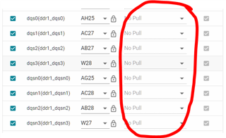
- If Option A is desired, two DDR3 devices must be mounted and external DQS and DQSn PU/PD must be not fitted
- If Option B is desired, high-word DDR3 memory must not be fitted and the external PU/PD of the DQS and DQSn connected to it must be fitted
Therefore, the PCB must contain to possible paths for this signals
- Path for Option A: DRA to DDR3 device and to a not fitted PU/PD
- Path for Option B: DRA to PU/PD and to a not fitted DDR3 device
I have reviewed the layout recommendations and I have not seen anything related with this scenario, so the question is:
¿Has TI any layout recommendation for DQS and DQSN lines taking into account their path is "splitted" between DDR3 and PU/PD?
PS: This question also applies to DRA777 and DRA750
Thank you very much in advance.