


Tool/software: Linux
Hi expert:
We are design J6-eco (DRA726) connect to VIN2A input 24bits RGB data to J6-eco.
Attached are the pin assign list and VIN1A schematic.
Now customer report that they just can input VIN1A_D8 - VIN1A_D23. All VIN1A_D0- VIN1A-D7 signal can not input to J6.
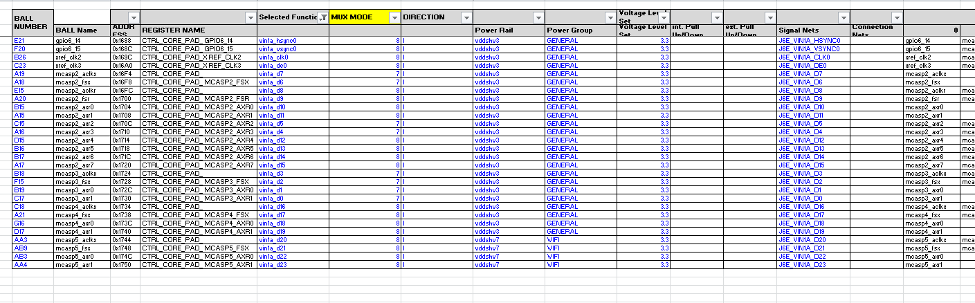
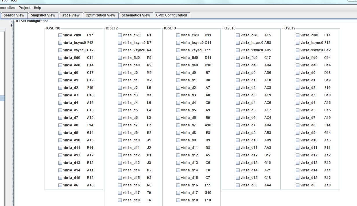
I have checked TRM 18.4.6.1.1 Table 18-6. Customer configure CTRL_CORE_VIP_MUX_SELECT[6:4] VIP_SEL_1A bit set to 0x3.
They use VIP1A group4A pin mux. VIN1A_D8-VIN1A-D23 pin muxmod is 0x8.
But VIP1A_D0-VINP1A_D7 pin belong Group6A. CTRL_CORE_VIP_MUX_SELECT[6:4] VIP_SEL_1A can not set as Group4A and Group6A work at the same time.
I believe customer need change their schematic and use another interface of VIN1A_D0-D23 configure.
Their schematic connect of VIN1A_D0 ~ VIN1A_D7 is wriong.
Please help me check wehther my understand is right.
Best Regards!
Han Tao
Below are their pin mux configure and schematic.


