This thread has been locked.

If you have a related question, please click the "Ask a related question" button in the top right corner. The newly created question will be automatically linked to this question.

AM4378: DDR3 invert_clockout flag criteria differs in excel tool from CCS GEL

Part Number: AM4378

Dear sirs,

Recently, we have had an issue related with the invert_clockout flag belonging to the DDR controller of our AM437x.

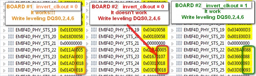
We have our “custom” board with an AM4378 and a couple of DDR3 (MT41J128M16JT-125 IT) in fly-by topology running at 400MHz.

Now, we have assembled 52 boards and more than 20% of these have not passed the initial DDR3 tests, so, after completely dismiss an assembling problem we have checked the DDR3 controller registers.

In the initial parameters for our own board and till today we have used the invert_clockout = 0 as a recommendation of the TI GEL for the AM437x, but, by the other hand, these days we have realized that a new excel tool “SPRAC70_AM437x_EMIF_Configuration_Tool_V20”(April 2017) recommends using (for our system) invert_clockout = 1.

Initially in 2016, we characterized the uboot memory controller using the available excel tool at that moment: “AM43xx_DDR_register_calc_tool”(2015)

That tool let configure 4 registers and no more.

SDRAM_CONFIG - SDRAM_TIMING_1 - SDRAM_TIMING_2 and SDRAM_TIMING_3

For the rest of registers, we used the characteristics of the AM437x “GEL” for the Code Composer Studio available on the web: http://processors.wiki.ti.com/index.php/File:AM437x_GELs.zip

The code in the GEL “says” that if DDR_CK length >= DDR_DQS length then the clock is not inverted, else the other config must be used.

#define DDR3_PHY_CTRL       0x00008009    //enable h/w training

                                                                       //invert_clkout=0 (if (DDR_CK length) >= (DDR_DQS length))

                                                                       //disable half delay mode

                                                                       //phy_dis_calib_rst set to 0

                                                                        //RD_Latency = (CL + 2) - 1

                                                                        //read latency of 7 for 400MHz

                                                                        // hwlvmod RD_Latency = CL+3 ; 9 for 400MHz                  

                                                                        // hwlvmod PHY_DLL_LOCK_DIFF incresed to 32- 0x00008xxx from 16 - 0x00004xxx


//#define DDR3_PHY_CTRL    0x00048009    //invert_clkout=1 (if (DDR_CK length) < (DDR_DQS length))                                                                                                                                                                        


Then, due our DDR_CK length is larger than DDR_DQS length we used the option “invert_clockout = 0” to config the EMIF4D_DDR3_PHY_CTRL. Moreover to be coherent with the invert_clockout option, we also programmed the EMIF4D_EXT_PHY_CONTROL_1 according to the GEL

#define PHY_CTRL_SLAVE_RATIO     0x80       // if invert_clkout = 0

//#define PHY_CTRL_SLAVE_RATIO   0x100      // if invert_clkout = 1

WR_MEM_32(EXT_PHY_CTRL_1, (PHY_CTRL_SLAVE_RATIO<<20)|(PHY_CTRL_SLAVE_RATIO<<10)|(PHY_CTRL_SLAVE_RATIO<<0));


Now, the new tool “SPRAC70_AM437x_EMIF_Configuration_Tool_V20”(2017 april) contemplates many more parameters (type of DDR3, type of system and PCB layout) and really gives a lot of more registers. But despite the DDR_CK length in our board continues being larger than DDR_DQS length (the PCB has not changed), the tool says that for our board must have invert_clockout at 1 instead of 0.

Really, with invert_clockout = 1 at both registers EMIF4D_DDR3_PHY_CTRL and EMIF4D_EXT_PHY_CONTROL_1 all our failing boards now functions.

Therefore, we are going to change our SW, but we have some questions:

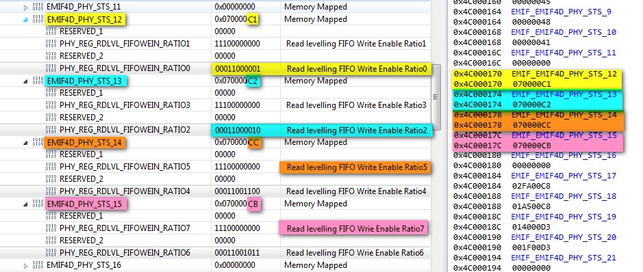
1)      Is there some merit factor (as a registers) that can be polled to verify that hardware leveling is locked at the right point? There is the EMIF4D_PHY_STS_X collection but didn’t exist detailed documentation about what it means or how to interpret it.

2)      It seems that the invert_clockout flag in EMIF4D_DDR_PHY_CTRL_1 is directly related with the value programmed in EMIF4D_EXT_PHY_CTRL_1, but there is no information about what this value means, except that this is the “ctrl slave ratio”(spruhl7d.pdf). I guess, this is like an initial seed for the convergence of DLL HWleveling algorithm, but it is supposition. We would like to have a detailed explanation about it.

3)      Regarding to the necessity of the use of invert_clockout = 1 instead of invert_clockout = 0 in designs where DDR_CK length is larger than DDR_DQS length I would like you to confirm that it is a limitation of the granularity of the DDR3 DLL controller.

Although it is not explained, I guess that the AM4378 DDR3 hwleveling controller has a “granularity” or a minimum degrees (or picoseconds) correction capacity, in most of the cases, bigger than the (CK vs DQS) ps PCB difference to be corrected, and due to this minimum granularity, the AM4378 uses the “invert_clock” technics. I suppose that’s because, emitting the inverted clock from the AM4378 is like an emulation of a larger PCB skew between (CK vs DQS) just to exceed these minimum picoseconds granularity of the AM4378 DDR3 DLL controller. But it is only a supposition. Please confirm it.

4)      Assuming that the values of our PCB are right introduced we would like if you were so kind to check it. We are going to launch the production and we don’t want new surprises.SPRAC70_AM437x_EMIF_Configuration_Tool_V20_modified_by_JFC.xlsx5807.2Gb_1_35V_DDR3L.pdf

  • Hi Jordi,

    you are correct in noticing that our recommendation and procedure for configuration of the DDR controller and PHY has changed since 2015.  We created the AM437x EMIF Configuration Tool to be a more comprehensive way of helping customers configure the DDR, so we currently recommend all customers to use this tool for their specific board designs.  The GEL file is specific to the EVMs TI provides and the values in that file may not be applicable to a custom design.  Here are some answers to your specific questions:

    1) You will see in the GEL that there is a status register which is checked to see if the hardware leveling completed without errors, but there is no hardware status to gauge the robustness of the results.  It is up to the customer to perform stress tests to ensure the robustness of the configuration.  

    The PHY_STS_X registers provide the results of the hardware leveling per byte, but we don’t provide all the details in the TRM.  As an example, the highlighted portions of the PHY_STS registers below show the results indicating the delay associated with aligning the DQS and CK signal to each of the 4 bytes on one of our evaluation boards.  The increasing values correspond to the placement in the fly-by topology on the board.

    4c000164: 00000044 00000044 00000000 07000033    

    4c000174: 0700004a 0700005d 07000071 00000000

    2) The ctrl slave ratio is associated with the launch timing of the Read DQS signal.  This value should be programmed as dictated by the spreadsheet and not modified

    3) Not really.  It is associated with the successful convergence of the h/w leveling in the controller.  We found that as long as the design layout guidelines from the device datasheet are followed, this invert_clkout setting will result in successful completion of the h/w leveling performed for all designs.  An invert_clkout=0 will also work for many designs, but invert_clkout=1 shifts the clock by half a cycle and gives better margin for the h/w training process.  The granularity you are talking about is represented in the status register mentioned above, with each value representing a fraction of the clock to delay the signal.  

    4) I reviewed the spreadsheet and uploaded my edits.  Double check the DDR Timings tabs for some edits i made based on the datasheet you provided.  There are some minor changes that need to be made.SPRAC70_AM437x_EMIF_Configuration_Tool_V20_modified_by_JFC_JamesEdits.xlsx

    Regards,

    James

  • Hi James,

    Thanks you so much for your rapid response.

    1) Yes, you are right and we understand that not all the parameters of an EVK must be usefull for a custom borad, but the EVK must be a starting point to beguin a custom design when there is no detailet information about some tricks to implement. Now, but with this new usefull tool that manages the invert_clockout, that's fine, despite the comment is there, in the GEL.

    Anyway, regarding the PHY_STS_X. I have decoded your information in my CCS. Really is it the DQS vs CK?.

    By the other hand I have encountered differences in PHY_STS_22, 23, 24 and 25 between boards ok (with invert_clkout = 0) vs boards ko (with clock_invertout = 0) and recobered boards ok with invert_clkout = 1. But, Is it really the write leveling difference of DQS vs CK?

    Please, see the picture of the writeleveling DQS ratios. The write levelling DQS ratio4 seems overflowed using the failing option, but there is no information of how interpret it or wich is the maxium acceptable level for this ratio. The failing board #number2 when has invert_clkout =1 functions and seems locekd at a medium point... 

    2) Ok for the 2 point.

    3) Ok for the 3 point.

    4) Regarding to your review of our EMIF parameters for our DDRs I've seen you've changed the tFAW, tRRD and tRFC. Please see my comments

    a) You have corrected tFAW to 50ns but I see in the datasheet (page 81) tFAW 40ns for DDR3L-1600 x16. Then I interpret it as 40ns. Is it right?

    b) You have corrected tRRD to 4CK and 10ns but I see in the datasheet (page 31) tRRD 6CK for DDR3L-1600 x16 and I also see in the datasheet (page 81) tRRD -> MIN = greater of 4CK or 7.5ns for DDR3L-1600 x16. Then I interpret it as 6CK and 7.5ns. Is it right?

    c) You have corrected the tRFC to 160ns and I agree since sheet values are per die and not per the whole memory.

    Thank you for your time

    Jordi Farré

  • 1) I think you are seeing why we switched to invert_clkout=1. The controller in some situations has trouble converging during h/w leveling with invert_clkout=0. The values you show look reasonable (0xC1/0xC2 for one memory, 0xCC/0xCD for other x16 memory). The values in STS_22-25 (which are associated with write DQS) should have a similar relationship. You can see that in the failing case, a value of 0x5/0x107 doesn't make sense. In the passing cases, the values look reasonable (ie. values are similar for bytes 0/1 and 2/3, since you have two 16 bit devices).

    4)
    a) you are right, i was looking at the wrong column. You should use tFAW=40ns
    b) you should be using the value on pg 81. Again, i was looking at the wrong column, so it should be using 4CK or 7.5ns

    Regards,
    James
  • Hi James,

    Thank you for your feedbacks.

    4a) and 4b) Ok, don`t worry. Thanks,

    Regarding to 1) I think there isn't enough information about the meaning and the convergence of these counters or values in PHY_STS_X and I suppose because it is reserved information?... I deduced "empirically" that the values in PHY_STS_23 where wrong in the failing board and now as you say I know that the values must to be similar, but again there is no information about the maximum or the minimum, etc.

    If you were so kind, could you provide more detailed information about the PHY_STS_Xs of the EMIF4D?

    Many thanks

  • Hi Jordi, all the values are 10-bits and represent the fraction of the clock cycle in units of 256ths in which the a signal will be delayed (depending on which group of STS regs you are looking at).

    So in your example above PHY_STS_22/23=0x88, which is a little over half a clock cycle (with an inverted clock, so really the delay is only about 8/256 of a clock). Note that the working version with invert_clkout=0, the value agrees (0x3 or 0x5). Since PHY_STS_24/25=0x93, that memory's trace lengths must be a little longer and require a little more delay.

    Regards,
    James
  • Hi James,

    Thanks for your time and your feedbacks.

    Jordi Farré