This thread has been locked.

If you have a related question, please click the "Ask a related question" button in the top right corner. The newly created question will be automatically linked to this question.

AM3871: DDR3 design questions

Other Parts Discussed in Thread: AM3871, TPS51200

Hello TI Experts,

I studied a few notes on the DDR3 memory layout from TI (SPRABI1C), NXP, Micron, Xilinx, and other manufacturers, and I had some questions:


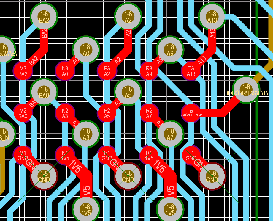
1. To which signal group does the DDR3.RESET signal (T2 pin in FBGA-96) belong to ADDR / COMMAND or CONTROL and is it necessary to match the length of this signal according to the length of the signals in one of these two groups or is it completely independent of the groups and length alignment?
2. Everywhere it is said that the length of the clock signals of the differential pair CK_P & CK_N should be 5 mil longer than the maximum length of the data bank signals?

For example, take one memory module with two banks BANK0 and BANK1:
BANK0 - length matching in group (difference 20 mil) - max.length for all signals in group is = 17.04mm
BANK1 - length matching in group (difference 20 mil) - max.length for all signals in group is = 31.84mm

Question:
What should be the length of the minimum length of the differential pair CK_P & CK_N?

Answer:
The minimum length of the differential pair is CK_P & CK_N = 32.34mm (maximum data signals length of banks (31.84mm) + 5mil).

Are my calculations and guesses correct?

3. My design program (Altium), when adding an impedance calculation profile, uses several reference planes (# 2 and # 4) for conductors (# 3) located on the inner layers of the board.

===========================
# 2 Ground Plane - Inner Layer
===========================
# 3 High Frequency - Inner Layer
===========================
# 4 Power Plane - Inner Layer
===========================

Questions:
a. Is it true that the supporting plane is always the same? (either above or below)
b. Will the split plane of the plane on the layer (# 4) affect the layer with conductors (# 3) if I choose the plane (# 2) as the only reference plane based on our communication in this topic? Or will both planes have an impact?

  • Please post what TI processor is this.
  • AM3871 (ARM Cortex-A8) with DDR3-1066.
  • Thanks,

    The relevant document is the device datasheet: www.ti.com/.../am3871.pdf The DDR3 routing specifications are in section 9.13.4.2. On to your questions:
    1. DDRx_RST does not belong to any class. This signal does not need to be length matched.
    2. The DDR_CLK differential traces need to be length matched to the ADDR/CTRL net class. See section 9.13.4.2.4.13.1. The DQS differential traces need to be length matched to the corresponding DQ net class. See section 9.13.4.2.4.13.2.
    3. Your PCB stackup is such that the DDR traces will be of the stripline type. Both planes will influence the trace impedance, depending on the dielectric type and thickness. It is highly undesirable to have split planes on the reference layers. See section 9.13.4.2.4.4.
  • Thank you. Everything is clear now.
  • 1. Does it make sense in the gaps between the memory conductors of the 50th (3W), if the distance is reduced to the minimum allowable 0.1mm in the area of ​​the contact pads, at the points where the trails pass near the vias? (screenshot 50ohm.png)
    2. What is the maximum difference in the lengths of the conductors between the groups BANK0, BANK1? Example: in my group the length of the conductors is aligned to 17mm, in the other to 31mm. Is this difference critical and do you need to align both groups to a certain average value?
    3. In some documents, some processor manufacturers said that the maximum difference in length between DQS0 / DQS0 #, DQS1 / DQS1 #, DQS2 / DQS2 #, DQS3 / DQS3 and CK / CK # should be no more than 500mil. Is this requirement adequate and is compliance really necessary?

  • 1. This isn't specifically mentioned for this device, however on newer processors we have: "Center-to-center spacing is allowed to fall to minimum (w) for up to 1250 mils of routed length", so I suppose this will be valide here too.
    2. There is no such requirement. Each data lane has its own control signals (DM, DQS), so there is no need to match lengths across data lanes.
    3. See No.2 above.
  • 1. My ADDR_CMD / CK length is 46.75mm, which is 1840mil and it is more than 1250mil pipe length to use the minimum clearance. How critical in my case would be a 4mil gap, with a conductor width of 6.5mil (for Outer Layers) and 4.5 (for Inner Layers)? What is the optimal gap value for my situation (for outer and inner layers)?
    2. Accepted
    3. Accepted

  • You may have issues with crosstalk between adjacent traces. Optimal conductor spacing is 4w center-to-center.
  • I now have a gap value of 4mil for all layers.

    My settings:
    for Outer Layers: trace width 6,5mil
    for Inner Layers: trace width 4,5mil

    Question:
    What is the value of the gap I choose to avoid problems with crosstalk?

  • Optimal conductor spacing is 4w center-to-center. The trace width on your outer layers seems a bit big. You could use 4-5mil traces on the outer layers if you modify the stackup, e.g. use thinner dielectric between the outer layes and layers below them.
  • I already use the minimum thickness of the dielectric for all layers. Core (construction: 2x (# 1506) 0.305mm), Prepreg (construction: 1x (# 106) 0.051mm). The width of the conductors with an impedance of 50 ohms and a tolerance of 10%. That is, do you still advise me to use 4mil clearance with the signal length group ADDR_CMD / CK 1840mil?

    My PCB manufacturer does not have other materials available, or they are already significantly more expensive than standard FR-4 TG130.

  • I am sorry, I don't see how we can help with this. I am attaching a stackup that I have used, that needs 4.75mils on outer layers and 5.25mils on inner layers. Drill holes are 0.2mm with 16-20mils vias (I don't remember the exact via size).

    Stackup.pdf

  • As far as I know, most manufacturers prohibit the use of 1 prepreg in the design of the board.


    The design of the board often consists of:
    2 prepreg
    1 core
    2 prepreg

    With such a stack like yours, a high probability of manufacturing defects.You also use the expensive FR-4 material with a high glass transition temperature TG150-170 of the Dk value, the Df of which is usually lower than that of my TG130 material.

    I am afraid only of crosstalk and therefore I do not know what kind of gap I should choose for my conductor widths.

  • I am sorry, we cannot confirm that a PCB layout, which does not conform to TI requirements will work or not. You should probably perform SI analysis to confirm your design.
  • In some notes from Xilinx, they recommend matching the length of the CONTROL group with the length of the CK group in addition to the ADDR_CMD group. Is it required at a speed of 1066 MT / s?
  • CK and ADDR_CTRL are considered a single group in the AM387x DDR3 routing guidelines. They should be matched as per Table 9-75.
  • First question:

    Figure 9-60 (Rcp, Cac) , Figure 9-61 (Rtt)
    In these figures, are these Rcp, Cac & Rtt components necessary only when using 4 memory modules? For two or less, this is not required?

    Found an error:
    Figure 9-58, Figure 9-59 - Lacked in the specification.

    Second question:

    8.2.9.2 Digital
    Pay special attention not to put so much capacitance on the supply that it slows the start-up voltage ramp
    enough to change the power sequencing order. Also be sure to verify that the main chip reset is low until
    after all supplies are at their correct voltage and stable.

    Table 9-71. Bulk Bypass Capacitors Per DDR3 EMIF
    DDR_1V5 bulk bypass total capacitance 70 μF (min)

    If I use TPS563200DDCT with 3 output filter capacitors of 22uF (66uF) to get 1V5, and also use 3x22uF as bulk capacitors as shown in table Table 9-71, will this violate the rule of section 8.2.9.2 Digital?

  • Q1: See Figure 9-54 and Figure 9-55. The terminations are required for all use cases. About the missing figures you can report using the "Submit Documentation Feedback" on the bottom of each page of the PDF document.

    Q2: No. Output filter capacitor must be placed close to the PMIC, and bulk capacitors need to be placed close to the DDR memories.
  • Mircon TN-46-14:
    Parallel termination is only used with DDR and only required where at least one of the
    following is true:
    • Five or more DDR devices
    • >2in (5cm) trace lengths
    • Poor simulation results
    • Single- or multibit errors during prototyping (after simulation)

    The problem is that for parallel termination a separate controller is needed, the power supply of which requires a voltage of 3.3V and a load current of about 800ma ~ (for example: TPS51200). In addition, additional free space is required for PCB wiring and regulator components and capacitors in accordance with the requirements of Micron (4–7µF) and two bulk capacitors (100µF) at each end.). In my situation, I’m breaking only one requirement, these are> 2in (5cm) trace lengths. I understand that it is more profitable for me to shorten the lengths of the conductors, rather than resorting to parallel termination. How do you think?
  • It's entirely your decision whether you will follow the TI design guidelines or not. TI will not discuss third-party documents. TI will also assume no responsibility if AM3871 datasheet requirements are not met.
  • Biser, thank you for your replies. Please tell me.
    Can I somehow, for example using a terminating serial resistor for example on the 50ohm, and having a conductor impedance of 75 ohm, reduce the conductor impedance to the 50ohm?

    Please look at example:

    Micron TN-41-13 (Figure 6 - Page 19)

    Please explain what happens to the impedance when this resistor is installed? In TI documents, sometimes there are terminating resistors 0-22ohm on the ADDR / CTRL / CMD bus. Explain their meaning and how does their installation affect the conductor impedance?

  • Series resistors are specifically prohibited on DDR3 signals in TI design recommendations. See Note 13 below Table 9-75 (datasheet page 303).
  • Thank for your replies,

    In some situations, it is required to separate Analog and Digital ground when using mixed signals. Based on what is written in the AM3871 specification, I see that this is not required.

    1. I want to understand why this requirement does not apply to this processor? Explain, please.

    I mean a similar scenario:

    2. I noticed that the DDR_VREF pins, as well as some USB-bus pins, such as USB0_DP, USB0_DM and others, have an analog signal type (A). Why is it that way?

    3. I cannot understand why a digital interface such as USB is marked in the documentation as an analog signal type (A)? Explain, please.

    4. Does this mean that they require the presence of an analog ground plane under the tracks for return currents where these signals pass?

    5. Is a solid reference plane needed for the power polygons on the inner layers? Does the gap in the plane on the adjacent inner layers if it intersects the polygon for example analog power on the adjacent inner layer?

  • Your last post is not directly related to the thread subject. Please open a new thread for it.
  • Hello Biser,

    I'm trying to choose a voltage regulator for DDR3 to generate VDDQ and I can’t understand what the optimal switching frequency should be in the case of dc-dc buck converter (step-down) and what it depends on. And shouldn't you use LDO instead of dc-dc buck converter for DDR3?

  • LDOs are slow and there may be voltage drops. Recommended power supply for DDR3 memory is buck converter.