This thread has been locked.

If you have a related question, please click the "Ask a related question" button in the top right corner. The newly created question will be automatically linked to this question.

AM3352: 32Gbit NAND flash options

Part Number: AM3352

Hello,

We are using am3352 with a SLC 8Gbit NAND flash. Now we need to include option for a 32Gbit NAND flash, but unfortunately we are not able to find a compatible NAND flash memry chip that fits the am335s requirements.

Main problem we are finding is pagesize, am3352 requires 2048/4096 pagesize, and available chips are 8192.

Could you please suggest compatible part numbers?

Our requirements are:

- Size: 32Gbit

- Temperature range: -40 to +85ºC

- One chip select

- 8-bit bus width

- TSOP48

- Technology: SLC preferred. MLC could be an option

Thank you for your help

Best regards

Angel

  • Hello Angel,

    My first thought is to use eMMC instead of NAND... or even an SD card. The capacities are typically larger than NAND and have none of the limitations like requiring upto 4K page size and requiring fewer than 16 ECC bits per 512byte block.

    Alternately, the GPMC has multiple chip selects that you could use with SLC NANDs that require only 4K page size.

    SLC is typically requried due to ECC limitation of 16 bits. Most MLC require > 16 bits for ECC.

    A search on Digikey turned up only one SLC 32Gb NAND, but it appears to use 4K pages. May be worth checking out (though I do not see any mention of ONFI compatibility)... media.digikey.com/.../TH58NVG5S0FTA20.pdf

    Do you need to boot from NAND? BCH16 ECC correction is used in ROM code.

    Refer to these similar posts...

    e2e.ti.com/.../674243
    - the GPMC/ELM is not able to support 8K pages, so we recommend using 4K-page parts with AM335x.


    e2e.ti.com/.../548804
    - BCH16 ECC correction in ROM code
    - 16Gb (2GB)

    processors.wiki.ti.com/.../Linux_Core_NAND_User's_Guide
    GPMC NAND driver supports:
    NAND devices having:
    bus-width = x8 | x16
    page-size = 2048 | 4096
    block-size = 128k | 256k
    1-bit Hamming, BCH4, BCH8 and BCH16 ECC schemes.

    e2e.ti.com/.../343017
    - 2 NANDs in a DTS file

    Regards,
    Mark
  • Hello Mark,

    Thank you very much for your response.

    Regarding using eMMC instead of NAND SLC we decided to use last one due to data reliability. Do you think it is possible to get the same data reliability using eMMC?

    We knew about that Toshiba memory, but it needs two chip selects and two wait pin signals, and our hardware is designed to use one chip select memory. Do you know any option with only one chip select?

    Anyway we have tried this memory, we can wire one spare pin to the second chip select but we have no option to wire the second wait signal.

    Best regards
    Angel
  • Hi Angel,

    eMMC is managed NAND - its controller handles the ECC, bad block management, and wear leveling for you, offloading this task from the CPU.

    eMMC likely uses MLC instead of SLC NAND, which might have different endurance and number of write cycles compared to SLC. Memory manufacturers will have better reliability information and might offer SLC NAND inside the eMMC for reliability concerns (I dont know).

    What specifically do you see as reliability concerns of eMMC verses raw NAND?

    I have heard complaints that eMMC can introduce less-deterministic latency compared to raw NAND with the controller between memory and the processor (imagine it detects ECC errors or a bad block and needs to move data around behind the scenes).

    Generally, the advantages of eMMC (larger capacity, fully managed) outweigh those of raw NAND. We run file systems on eMMC in many of the EVMs we offer.

    =-=-

    If you choose to use the NAND with 2 chip selects, but only have one CS routed from the processor... I can conceive of some glue logic to share the single CS across 2 CS inputs of the NAND...
    * GPIO controlled external mux - use 1 GPIO to select a 2-1 mux to route the single CS to either CS0 or CS1

    2-input OR gates with a GPIO and 1 CS as inputs. Connect the output to the CS input on the NAND (when GPIO is low, the active low CS will pass through) - requires 2 GPIOs for 2 CS inputs (or an inverter before one of the OR gates to use the same GPIO pin - high passes CS to one CS input, low passes CS to the other CS input)

    I would avoid using the GPIO as a CS because it will leave the devices selected more than necessary.

    See this similar post. It is the inverse of this problem where multiple EMIF CS pins are routed through glue logic to address pins, but the approach is similar...
    e2e.ti.com/.../2829884

    Hope this helps,
    Mark

  • Hello Mark,

    Thank you very much for your response.

    Finally we managed to wire manually both chip selects and both wait pin signals, and now we are trying to program the memory.
    We use kernel 4.14.67 got from TI SDK. We have changed OOB size calculation in function nand_decode_ext_id() inside nand_base.c

    Original code is:
    /* Calc oobsize */
    mtd->oobsize = (8 << (extid & 0x01)) * (mtd->writesize >> 9);
    This leads to a OOB size value of 128 and starting system from SD, when it detects the NAND flash we get this error
    [ 1.967167] omap2-nand 8000000.nand: not enough OOB bytes required = 210, available=128

    To avoid this we set OOB size to 232 for this memory(as stated in datasheet) and now memory is detected properly and partitions are created for both chip selects as defined in our .dts file. The problem is when we want to program the NAND flash.

    root@arm:# mtdinfo /dev/mtd0
    mtd0
    Name: NAND.SPL
    Type: nand
    Eraseblock size: 262144 bytes, 256.0 KiB
    Amount of eraseblocks: 2 (524288 bytes, 512.0 KiB)
    Minimum input/output unit size: 4096 bytes
    Sub-page size: 1024 bytes
    OOB size: 232 bytes
    Character device major/minor: 90:0
    Bad blocks are allowed: true
    Device is writable: true

    root@arm:# flash_erase /dev/mtd0 0 0
    Erasing 256 Kibyte @ 40000 -- 100 % complete

    root@arm:# nandwrite -p /dev/mtd0 MLO
    Writing data to block 0 at offset 0x0
    [ 558.073024] ------------[ cut here ]------------
    [ 558.078187] WARNING: CPU: 0 PID: 291 at drivers/mtd/nand/nand_base.c:1070 nand_wait+0x110/0x118
    [ 558.090208] Modules linked in: musb_dsps musb_hdrc udc_core usbcore phy_am335x phy_generic usb_common phy_am335x_control c_can_pla
    tform c_can mcp251x can_dev snd_soc_tlv320aic31xx musb_am335x omap_wdt sd8xxx(O) mlan(O) cfg80211 ppp_generic slhc owa4x_gpio
    [ 558.115334] CPU: 0 PID: 291 Comm: nandwrite Tainted: G O 4.14.67-1.0.6+ #46
    [ 558.123823] Hardware name: Generic AM33XX (Flattened Device Tree)
    [ 558.130205] Backtrace:
    [ 558.132793] [<c010c01c>] (dump_backtrace) from [<c010c2ec>] (show_stack+0x18/0x1c)
    [ 558.140729] r7:00000009 r6:60070013 r5:00000000 r4:c0e57724
    [ 558.146674] [<c010c2d4>] (show_stack) from [<c08eb924>] (dump_stack+0x8c/0xa0)
    [ 558.154256] [<c08eb898>] (dump_stack) from [<c012a3f8>] (__warn+0xec/0x104)
    [ 558.161553] r7:00000009 r6:c0c51370 r5:00000000 r4:00000000
    [ 558.167489] [<c012a30c>] (__warn) from [<c012a4c8>] (warn_slowpath_null+0x28/0x30)
    [ 558.175424] r9:dc7d0000 r8:00001000 r7:000064f7 r6:c0e02d00 r5:dc5ff810 r4:00000080
    [ 558.183544] [<c012a4a0>] (warn_slowpath_null) from [<c0602ab8>] (nand_wait+0x110/0x118)
    [ 558.191934] [<c06029a8>] (nand_wait) from [<c0601848>] (nand_do_write_ops+0x39c/0x504)
    [ 558.200230] r7:00000000 r6:c0602b08 r5:00001000 r4:dc5ff810
    [ 558.206161] [<c06014ac>] (nand_do_write_ops) from [<c0601a14>] (nand_write+0x64/0x84)
    [ 558.214369] r10:00001000 r9:00000000 r8:00004000 r7:dc7d0000 r6:db529e84 r5:db529db8
    [ 558.222570] r4:dc5ff810
    [ 558.225233] [<c06019b0>] (nand_write) from [<c05f7a9c>] (part_write+0x48/0x50)
    [ 558.232804] r10:dc7d0000 r9:db528000 r8:00000000 r7:00000000 r6:b6e36008 r5:00000000
    [ 558.241005] r4:00000000
    [ 558.243662] [<c05f7a54>] (part_write) from [<c05f4138>] (mtd_write+0x88/0xa0)
    [ 558.251137] r5:00000000 r4:c05f7a54
    [ 558.254888] [<c05f40b0>] (mtd_write) from [<c05fad18>] (mtdchar_write+0xc0/0x23c)
    [ 558.262730] r7:db529f80 r6:b6e36008 r5:00001000 r4:00001000
    [ 558.268672] [<c05fac58>] (mtdchar_write) from [<c0247180>] (__vfs_write+0x34/0x134)
    [ 558.276697] r10:00000000 r9:00001000 r8:db529f80 r7:db529f80 r6:b6e36008 r5:c05fac58
    [ 558.284896] r4:db06f840
    [ 558.287554] [<c024714c>] (__vfs_write) from [<c0247404>] (vfs_write+0xac/0x170)
    [ 558.295214] r10:00000000 r9:db528000 r8:c0108084 r7:db529f80 r6:b6e36008 r5:db06f840
    [ 558.303414] r4:00001000
    [ 558.306071] [<c0247358>] (vfs_write) from [<c02475f8>] (SyS_write+0x4c/0xa8)
    [ 558.313458] r9:db528000 r8:c0108084 r7:00001000 r6:b6e36008 r5:db06f840 r4:db06f840
    [ 558.321581] [<c02475ac>] (SyS_write) from [<c0107ea0>] (ret_fast_syscall+0x0/0x54)
    [ 558.329510] r7:00000004 r6:bea11b78 r5:00000000 r4:00000000
    [ 558.345023] ---[ end trace 17e2261adde1eb6c ]---
    [ 558.354826] ------------[ cut here ]------------
    [ 558.361008] WARNING: CPU: 0 PID: 291 at drivers/mtd/nand/nand_base.c:1070 nand_wait+0x110/0x118
    [ 558.371006] Modules linked in: musb_dsps musb_hdrc udc_core usbcore phy_am335x phy_generic usb_common phy_am335x_control c_can_pla
    tform c_can mcp251x can_dev snd_soc_tlv320aic31xx musb_am335x omap_wdt sd8xxx(O) mlan(O) cfg80211 ppp_generic slhc owa4x_gpio
    [ 558.395642] CPU: 0 PID: 291 Comm: nandwrite Tainted: G W O 4.14.67-1.0.6+ #46
    [ 558.404125] Hardware name: Generic AM33XX (Flattened Device Tree)
    [ 558.410506] Backtrace:
    [ 558.413089] [<c010c01c>] (dump_backtrace) from [<c010c2ec>] (show_stack+0x18/0x1c)
    [ 558.421024] r7:00000009 r6:60070013 r5:00000000 r4:c0e57724
    [ 558.426967] [<c010c2d4>] (show_stack) from [<c08eb924>] (dump_stack+0x8c/0xa0)
    [ 558.434547] [<c08eb898>] (dump_stack) from [<c012a3f8>] (__warn+0xec/0x104)
    [ 558.441842] r7:00000009 r6:c0c51370 r5:00000000 r4:00000000
    [ 558.447775] [<c012a30c>] (__warn) from [<c012a4c8>] (warn_slowpath_null+0x28/0x30)
    [ 558.455708] r9:dc7d0000 r8:00001000 r7:00006513 r6:c0e02d00 r5:dc5ff810 r4:00000080
    [ 558.463824] [<c012a4a0>] (warn_slowpath_null) from [<c0602ab8>] (nand_wait+0x110/0x118)
    [ 558.472211] [<c06029a8>] (nand_wait) from [<c0601848>] (nand_do_write_ops+0x39c/0x504)
    [ 558.480506] r7:00000000 r6:c0602b08 r5:00001000 r4:dc5ff810
    [ 558.486436] [<c06014ac>] (nand_do_write_ops) from [<c0601a14>] (nand_write+0x64/0x84)
    [ 558.494642] r10:00001000 r9:00000000 r8:0000a000 r7:dc7d0000 r6:db529e84 r5:db529db8
    [ 558.502841] r4:dc5ff810
    [ 558.505502] [<c06019b0>] (nand_write) from [<c05f7a9c>] (part_write+0x48/0x50)
    [ 558.513071] r10:dc7d0000 r9:db528000 r8:00000000 r7:00000000 r6:b6e3c008 r5:00000000
    [ 558.521270] r4:00000000
    [ 558.523926] [<c05f7a54>] (part_write) from [<c05f4138>] (mtd_write+0x88/0xa0)
    [ 558.531399] r5:00000000 r4:c05f7a54
    [ 558.535149] [<c05f40b0>] (mtd_write) from [<c05fad18>] (mtdchar_write+0xc0/0x23c)
    [ 558.542988] r7:db529f80 r6:b6e3c008 r5:00001000 r4:00001000
    [ 558.548929] [<c05fac58>] (mtdchar_write) from [<c0247180>] (__vfs_write+0x34/0x134)
    [ 558.556953] r10:00000000 r9:00001000 r8:db529f80 r7:db529f80 r6:b6e3c008 r5:c05fac58
    [ 558.565152] r4:db06f840
    [ 558.567809] [<c024714c>] (__vfs_write) from [<c0247404>] (vfs_write+0xac/0x170)
    [ 558.575469] r10:00000000 r9:db528000 r8:c0108084 r7:db529f80 r6:b6e3c008 r5:db06f840
    [ 558.583668] r4:00001000
    [ 558.586325] [<c0247358>] (vfs_write) from [<c02475f8>] (SyS_write+0x4c/0xa8)
    [ 558.593712] r9:db528000 r8:c0108084 r7:00001000 r6:b6e3c008 r5:db06f840 r4:db06f840
    [ 558.601834] [<c02475ac>] (SyS_write) from [<c0107ea0>] (ret_fast_syscall+0x0/0x54)
    [ 558.609764] r7:00000004 r6:bea11b78 r5:00000000 r4:00000000
    [ 558.625210] ---[ end trace 17e2261adde1eb6d ]---
    [ 558.631883] ------------[ cut here ]------------
    [ 558.636868] WARNING: CPU: 0 PID: 291 at drivers/mtd/nand/nand_base.c:1070 nand_wait+0x110/0x118
    [ 558.647531] Modules linked in: musb_dsps musb_hdrc udc_core usbcore phy_am335x phy_generic usb_common phy_am335x_control c_can_pla
    tform c_can mcp251x can_dev snd_soc_tlv320aic31xx musb_am335x omap_wdt sd8xxx(O) mlan(O) cfg80211 ppp_generic slhc owa4x_gpio
    [ 558.672243] CPU: 0 PID: 291 Comm: nandwrite Tainted: G W O 4.14.67-1.0.6+ #46
    [ 558.680725] Hardware name: Generic AM33XX (Flattened Device Tree)
    [ 558.687106] Backtrace:
    [ 558.689688] [<c010c01c>] (dump_backtrace) from [<c010c2ec>] (show_stack+0x18/0x1c)
    [ 558.697621] r7:00000009 r6:60070013 r5:00000000 r4:c0e57724
    [ 558.703563] [<c010c2d4>] (show_stack) from [<c08eb924>] (dump_stack+0x8c/0xa0)
    [ 558.711143] [<c08eb898>] (dump_stack) from [<c012a3f8>] (__warn+0xec/0x104)
    [ 558.718437] r7:00000009 r6:c0c51370 r5:00000000 r4:00000000
    [ 558.724370] [<c012a30c>] (__warn) from [<c012a4c8>] (warn_slowpath_null+0x28/0x30)
    [ 558.732303] r9:dc7d0000 r8:00001000 r7:0000652f r6:c0e02d00 r5:dc5ff810 r4:00000080
    [ 558.740420] [<c012a4a0>] (warn_slowpath_null) from [<c0602ab8>] (nand_wait+0x110/0x118)
    [ 558.748807] [<c06029a8>] (nand_wait) from [<c0601848>] (nand_do_write_ops+0x39c/0x504)
    [ 558.757102] r7:00000000 r6:c0602b08 r5:00001000 r4:dc5ff810
    [ 558.763032] [<c06014ac>] (nand_do_write_ops) from [<c0601a14>] (nand_write+0x64/0x84)
    [ 558.771237] r10:00001000 r9:00000000 r8:0000c000 r7:dc7d0000 r6:db529e84 r5:db529db8
    [ 558.779437] r4:dc5ff810
    [ 558.782099] [<c06019b0>] (nand_write) from [<c05f7a9c>] (part_write+0x48/0x50)
    [ 558.789669] r10:dc7d0000 r9:db528000 r8:00000000 r7:00000000 r6:b6e3e008 r5:00000000
    [ 558.797867] r4:00000000
    [ 558.800523] [<c05f7a54>] (part_write) from [<c05f4138>] (mtd_write+0x88/0xa0)
    [ 558.807995] r5:00000000 r4:c05f7a54
    [ 558.811745] [<c05f40b0>] (mtd_write) from [<c05fad18>] (mtdchar_write+0xc0/0x23c)
    [ 558.819585] r7:db529f80 r6:b6e3e008 r5:00001000 r4:00001000
    [ 558.825525] [<c05fac58>] (mtdchar_write) from [<c0247180>] (__vfs_write+0x34/0x134)
    [ 558.833549] r10:00000000 r9:00001000 r8:db529f80 r7:db529f80 r6:b6e3e008 r5:c05fac58
    [ 558.841749] r4:db06f840
    [ 558.844405] [<c024714c>] (__vfs_write) from [<c0247404>] (vfs_write+0xac/0x170)
    [ 558.852065] r10:00000000 r9:db528000 r8:c0108084 r7:db529f80 r6:b6e3e008 r5:db06f840
    [ 558.860265] r4:00001000
    [ 558.862922] [<c0247358>] (vfs_write) from [<c02475f8>] (SyS_write+0x4c/0xa8)
    [ 558.870310] r9:db528000 r8:c0108084 r7:00001000 r6:b6e3e008 r5:db06f840 r4:db06f840
    [ 558.878433] [<c02475ac>] (SyS_write) from [<c0107ea0>] (ret_fast_syscall+0x0/0x54)
    [ 558.886363] r7:00000004 r6:bea11b78 r5:00000000 r4:00000000
    [ 558.897996] ---[ end trace 17e2261adde1eb6e ]---


    Do you know what else we are missing?
    Best regards
    Angel
  • Hello again Mark,

    We start the system from the SD, stop at the bootloader and write the SPL and u-boot. We check that both files are flashed properly at the correct address.

    But the system does not start from NAND flash, and the result is as if the NAND flash is empty.

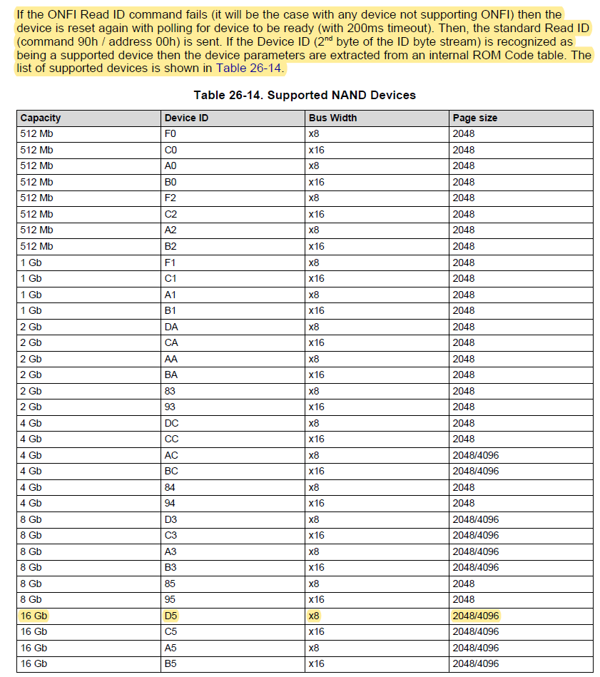
    I checked "Table 26-14. Supported NAND Devices" in the TRM document:
    Capacity Device ID Bus Width Page size
    32 Gb D7 x8 2048/4096
    32 Gb C7 x16 2048/4096
    32 Gb A7 x8 2048/4096
    32 Gb B7 x16 2048/4096
    32 Gb 87 x8 2048
    32 Gb 97 x16 2048

    The Toshiba memory device ID is 0xD5, and it is not included in the table.

    Could the problem be that this Toshiba memory is not supported by am335x processor?

    Best regards
    Angel
  • Hi Angel,

    Sadly that Toshiba part seems not to support ONFI, and it is not listed with the other supported NAND devices. So it might not be supported by the boot loader.

    I will confirm with a colleague and get back to you in a day or two.

    Regards,
    Mark

    [EDIT - Device ID D5 is listed on Table 26-14. Supported NAND Devices (as a 16Gb, x8, 2048/4096 device).

  • Hi Mark,

    Could you help to get a feedback on that case?

    Thanks in advanced.
    Regards,
  • Hi Angel,

    I checked Table 26-14 Supported NAND Devices, and it includes Device ID "D5"

    The Device ID maps to a 16Gb Capacity, x8 Bus Width, 2048/4096 page size.

    How are you programming the NAND? Did you get the NAND Flash Writer to run? What parameters did you pass when programming the NAND?

    Do you have any ability to capture waveforms with a scope during the NAND boot?

    Helpful E2E threads:

    https://e2e.ti.com/support/processors/f/791/t/207275

    - nand flash writer

    https://e2e.ti.com/support/processors/f/791/t/323432

    https://e2e.ti.com/support/processors/f/791/t/244832?AM335x-Android-NAND-Boot-issue

    Helpful Wikis:

    http://processors.wiki.ti.com/index.php/AM335X_StarterWare_Booting_And_Flashing#Flashing_bootloader_and_application_to_NAND_Flash

    http://processors.wiki.ti.com/index.php/AM335x_CCS_Flashing_Tools_Guide

    Regards,
    Mark

  • Hello Mark,

    Thank you very much for your help.
    You are right, ID D5 is in the table for 16Gb memories. This memory is a 32 Gb memory but internally they are two independent 16 GB memories.

    Our systems starts from external SD card if NAND flash is empty, so we are starting the system from SD. We changed the oobsize parameter calculation, both in bootloader and linux system, because calculation method leads to a value of 128

    mtd->oobsize = (8 << (extid & 0x01)) * (mtd->writesize >> 9);

    128 is a wrong value, so we change it to 232.

    We start system from SD and write NAND flash using bootloader commands (as we do with other NAND flash devices).

    => nand info

    Device 0: nand0, sector size 256 KiB
    Page size 4096 b
    OOB size 232 b
    Erase size 262144 b
    subpagesize 1024 b
    options 0x40000004
    bbt options 0x 8000
    =>
    => nand erase.part NAND.SPL

    NAND erase.part: device 0 offset 0x0, size 0x80000
    Erasing at 0x40000 -- 100% complete.
    OK
    => nand erase.part NAND.u-boot

    NAND erase.part: device 0 offset 0x280000, size 0x100000
    Erasing at 0x340000 -- 100% complete.
    OK
    => tftp 0x82000000 MLO
    link up on port 1, speed 100, full duplex
    Using ethernet@4a100000 device
    TFTP from server 192.168.100.154; our IP address is 192.168.100.42
    Filename 'MLO'.
    Load address: 0x82000000
    Loading: ######
    4.2 MiB/s
    done
    Bytes transferred = 74372 (12284 hex)
    CACHE: Misaligned operation at range [82000000, 82012284]
    => nand write ${fileaddr} NAND.SPL ${filesize}

    NAND write: device 0 offset 0x0, size 0x12284
    74372 bytes written: OK
    =>
    => tftp 0x82000000 u-boot.img
    link up on port 1, speed 100, full duplex
    Using ethernet@4a100000 device
    TFTP from server 192.168.100.154; our IP address is 192.168.100.42
    Filename 'u-boot.img'.
    Load address: 0x82000000
    Loading: #################################
    4.6 MiB/s
    done
    Bytes transferred = 481244 (757dc hex)
    CACHE: Misaligned operation at range [82000000, 820757dc]
    => nand write ${fileaddr} NAND.u-boot ${filesize}

    NAND write: device 0 offset 0x280000, size 0x757dc
    481244 bytes written: OK
    =>
    => nand read 0x82000000 0x00 0x800

    NAND read: device 0 offset 0x0, size 0x800
    OWASYS nand_do_read_ops ENTER
    2048 bytes read: OK
    => md 0x82000000
    82000000: 00000040 0000000c 00000000 00000000 @...............
    82000010: 00000000 45534843 4e495454 00005347 ....CHSETTINGS..
    82000020: ffffffff ffffffff ffffffff ffffffff ................
    82000030: ffffffff ffffffff ffffffff ffffffff ................
    82000040: c0c0c0c1 00000100 00000000 00000000 ................
    82000050: 00000000 00000000 00000000 00000000 ................
    82000060: 00000000 00000000 00000000 00000000 ................
    82000070: 00000000 00000000 00000000 00000000 ................
    82000080: 00000000 00000000 00000000 00000000 ................
    82000090: 00000000 00000000 00000000 00000000 ................
    820000a0: 00000000 00000000 00000000 00000000 ................
    820000b0: 00000000 00000000 00000000 00000000 ................
    820000c0: 00000000 00000000 00000000 00000000 ................
    820000d0: 00000000 00000000 00000000 00000000 ................
    820000e0: 00000000 00000000 00000000 00000000 ................
    820000f0: 00000000 00000000 00000000 00000000 ................
    =>

    As you can see NAND is written, and values are correct, but system can not start from flash.

    We can connect the a scope to the signals. What do you want us to check?

    Best regards and thank you
    Angel
  • Hello Angel,

    Can you apply the patch from this post and retry?

    Best regards,
    Kemal

  • Hello Kemal,

    I think it was applyed in our version

    flush_cache(load_addr, size);

    Anyway I changed as you said

    flush_cache(load_addr, ALIGN(size, ARCH_DMA_MINALIGN));

    But it did not work. I test it with a different memory chip reference and it does work as before.

    Best regards
    Angel
  • Okay. I just wanted to make sure that you have that patch applied.
  • Angel,

    Could you please let us know what version of U-Boot and Linux you are using? Which Processor SDK version? Thanks.
  • Hello,

    We are using u-boot version 2016.09-rc2, and linux version is 4.14.67 from TI SDK 05.01.00.11

    Best regards
    Angel
  • Angel,

    Why are you using such an old version of U-Boot? I would highly recommend you move to the 2018.01 version that also come with Processo SDK v5 and retry your NAND procedures.

    We can't actively support such an old version of U-Boot.
  • Hello,

    For changing to the new u-boot we need to port this new version to our hardware, and this would take us some time.
    We could do it, but we do not understand if this is going to solve this problem.

    u-boot version we are using works whit other NAND chips.

    It can run from a SD card, and also read and write this TOSHIBA memory. The problem is when the processor is trying to start-up from this TOSHIBA NAND flash. We see that the system is trying to start once and again but it is not able to start. The problem seems to be that the processor is not able to run from this NAND flash, not depending on which firmware is loaded on it.

    We do not see how changing u-boot will change this behavior.

    Best regards
    Angel
  • Angel,

    OK, I understand and agree that switching U-Boot versions won't help with this problem.

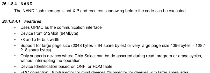
    We believe that this stems from the 8K page size of your NAND. From our TRM, Ch. 26, we only support 2K and 4K page sizes for booting:

    U-Boot and the Kernel can support 8K, but the boot ROM cannot per the above. We would recommend using some other boot media to get to U-Boot.

    I hope this addresses your issue.

  • Hello,

    The NAND we are trying is not 8K page size, it is 4K page size. Device code is TH58NVG5S0FTAK0, and this is what we can find looking at data sheet:

    DESCRIPTION
    The TH58NVG5S0F is a single 3.3V 32 Gbit (36,305,895,424 bits) NAND Electrically Erasable and
    Programmable Read-Only Memory (NAND E 2 PROM) organized as (4096 + 232) bytes × 64 pages × 16384 blocks.
    The device has two 4328-byte static registers which allow program and read data to be transferred between the
    register and the memory cell array in 4328-byte increments. The Erase operation is implemented in a single block
    unit (256 Kbytes + 14.5 Kbytes: 4328 bytes × 64 pages).
    The TH58NVG5S0F is a serial-type memory device which utilizes the I/O pins for both address and data
    input/output as well as for command inputs. The Erase and Program operations are automatically executed making
    the device most suitable for applications such as solid-state file storage, voice recording, image file memory for still
    cameras and other systems which require high-density non-volatile memory data storage.
    FEATURES

    Organization
    Memory cell array
    Register
    Page size
    Block size
    x8
    4328 × 256K × 8 × 4
    4328 × 8
    4328 bytes
    (256K + 14.5K) bytes

    Best regards
    Angel
  • Angel, are you able to connect to your board via JTAG?  It is not clear from the previous post where exactly the failure is occurring, whether in the ROM or SBL.  If you can connect thru JTAG, what is the program counter (PC) after a failure.  Also, can you run the Debug script described here:  http://processors.wiki.ti.com/index.php/AM335x_board_bringup_tips#Analyzing_Boot_Issues_with_CCS_and_JTAG

    so we can get more info on the failure.

    Thanks,

    James

  • Hello James,

    Sorry, but we do not have possibility to connect JTAG. As you suggested we have connected all NAND flash signals with the oscilloscope, do you want us to look for something specifically?

    One more difference we have noticed between working and not working NAND flash:
    1. Not working flash: If we flash a dummy file in the SPL partition, am3352 is not able to start and it is resetting and restarting every few seconds.
    2. Working flash: If we flash a dummy file in the SPL partition, am3352 is not able to start but it only try once. It is not resetting.

    With not working Toshiba NAND flash, situation is the same than if SPL partition is empty, not flashed.

    I hope this can help.
    Best regards
    Angel
  • Hi Angel,
    it will be difficult to debug this without JTAG access. Here are a few things to try.

    -boot from the SD card to get to a point where you can successfully read/write the NAND. Then remove the card and perform a cold reset and see if it can boot from the NAND. I just want to eliminate any possible power up issues during boot.
    -If you have a fairly deep memory on your scope, you can try to capture the first few command/response between the processor and memory, just to see how far the NAND boot goes. You should be able to see if it gets thru the identification stage, or maybe it is failing further into the boot.

    A few questions:
    -What is your boot order? What are your SYSBOOT signals?

    regards,
    James
  • Hi James,

    We have been analysing the communication with the scope and made good progress, we would like you to confirm from TI side that our conclusions are correct, and the options we have now.

    - SYSBOOT: 0100 0000 0001 0011 (ECC done by ROM, 8 bit device, NAND, NANDI2C, MMC0, UART0)

    When we boot from the microSD and read/write the NAND flash we see that it is correctly flashed and that it reads 26 ECC bytes after Reading the data.

    When we boot from the NAND flash, we see that only reads 14 ECC bytes after Reading the data. This made us think that it is using BCH-8 while we understand from the SPRUH73P (page 5046) that it should be BCH-16.

    For device ID codes D3h, C3h, D5h, C5h, D7h, C7h, DEh, CEh when manufacturer code (first ID byte) is 98h the Cell type information is checked in the 4th byte of ID data. If it is equal to 10b then the ECC correction applied is BCH 16b/sector.

    The sequence of operations from the NAND are:

    - Reset     FF

    - Id Read  90 20 98 D5 91 26   (98 Maker code, D5 Device code, 91 Chip Number, Cell Type, 26 Page Size, Block size) 

    - Reset     FF

    - Id Read  90 00 98 D5 91 26   (98 Maker code, D5 Device code, 91 Chip Number, Cell Type, 26 Page Size, Block size) 

    - Read      00 00 10 00 00 00 30     Data read FF

    .....

    From the 4th byte, 26 we understand that it should be BCH16 instead of BHC8.

    We have done the following tests to confirm the previous affirmation.

    - Connect Sysboot 9 to 1 -> ECC done by Flash -> This makes the bootloader to boot from NAND.

    - Change BCH 16 to BCH 8 in the uboot, and flash it to the NAND. -> This makes the bootloader to from from NAND

    Now we have the following questions:

    - Is it reading incorrectly the 4th byte and using? Does this mean that we can only use BCH-8 for bootloader?

    - Could we use BCH-16 to flash the Kernel and filesystem from the running bootloader? We have always used BCH-16 and we would like to keep it in the same way for reliability at least in the Kernel and Filesystem.

    - We have noticed that it takes about 3 times more (from 5 to 15 seconds) to start the bootloader. What could be the reason?

    Thanks a lot for your help

    Angel 

  • Angel,

    If it is reading 0x26 in the 4th byte, that means that bits [3:2] are 01b, which means the cell type is 4 levels, and the ROM will choose BCH-8 because of this (see table 26-15 in the TRM for the decode of the 4th byte).  It seems the NAND you are using only requires BCH-8.  Thus, that is what the ROM will choose.  

    You should be able to use BCH-16 for the rest of the NAND which the ROM doesn't read.  Or you can just choose the ECC to be performed by the flash.

    I'm not sure why the boot is taking 3 times longer.  Do you mean it takes 3 times longer with the new 32Gb NAND vs the smaller one?  Can you narrow down where the extra time is spent (eg, in ROM, u-boot, or booting kernel)?

    Regards,

    James

  • Hi James,

    Good to know the bits it is looking into to check for the 01b, we had assumed it was the lowest bits as it's not specified in the TRM.

    The problem seems to be that Toshiba's byte meaning is:

    What is being searched by the ROM in the 4th byte really is in the 3rd. We have checked D5 memories from Micron and Hynix and it seems that they have the same structure as Toshiba, so we don't see why it is being looked in the 4th byte. These bits [3:2] of the 4th byte are reserved in Toshiba and have information about spare page bytes or other info in other manufacturers. 

    Our NAND memory is SLC, 2 level cell so BCH-8 would be enough. The ECC needs to be done in the microprocessor as the memory does not have it.

    The boot time with this 2x16Gbit NAND SLC flash is 3 times longer than with 16Gbit MT29F16G08ABABAWP-AIT:B. This time is from power on to first uboot characters in terminal.

    Thanks

    Angel

  • Angel,

    I checked the ROM code, and it does use the SpareBytesPerPage parameter to determine the best ECC type.  It looks like you will have to stick with BCH8, at least for the portion read by the ROM.

    I don't have any good ideas as to why the boot time is so much longer.  In order to debug the long boot time, you would need to get a little more granularity in the boot process.  One way to do this is to insert GPIO toggles into different parts of MLO and/or u-boot, and monitor these toggles on a scope to check differences.  This will help you check if it is the ROM (measure POR release to first GPIO toggle), or somewhere in the MLO/u-boot.  

    Regards,

    James

  • Hello James,

    Thank you for checking at your side. Now it is clear and we will try to see the options we have.

    Regarding the booting time we will keep on making some tests, because adding these seconds to the start up could cause some problems in our systems.

    Best regards and thank you for your help

    Angel