This thread has been locked.

If you have a related question, please click the "Ask a related question" button in the top right corner. The newly created question will be automatically linked to this question.

AM3352: GPMC timing details

Part Number: AM3352

Hi  Champs,

I would like to confirm this AM3352 data sheet 

http://www.ti.com/lit/ds/sprs717k/sprs717k.pdf

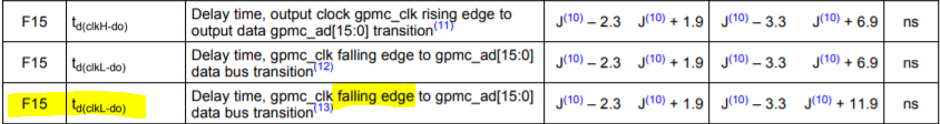
Table 7-24. GPMC and NOR Flash Switching Characteristics—Synchronous Mode has three "F15".

Each of F15 parameter has following  Note.

(11) First transfer only for CLK DIV 1 mode.

(12) Half cycle; for all data after initial transfer for CLK DIV 1 mode.

(13) Half cycle of GPMC_CLK_OUT; for all data for modes other than CLK DIV 1 mode. GPMC_CLK_OUT divide down from GPMC_FCLK.


<Question 1 >

Could you please explain what is "CLK DIV 1 mode" meaning on the above (11) , (12), (13) ?

Is this same as "GPMCFCLKDIVIDER" =1h mean ?

<Question 2> 

If  "CLK DIV 1 mode" indicate GPMCFCLKDIVIDER=1h,

we use GPMCFCLKDIVIDER =0h. So, Is this  meaning NOT "CLK DIV 1mode" ?

Then, we have to apply above (13)  ,right ?

If everything correct , we don't need refer all three F15 comment.

we can look into only one F15 with note 13,  right ?

<Question 3> 

We didn't understand this note (13) exact meaning. 

(13) Half cycle of GPMC_CLK_OUT; for all data for modes other than CLK DIV 1 mode. GPMC_CLK_OUT divide down from GPMC_FCLK.

F15 comment is "Delay time, gpmc_clk falling edge to gpmc_ad[15:0] data bus transition"

So, this "Delay time" is half cycle of GPMC_CLK_OUT that divide down from GPMC_FCLK, is this correct ?

<Question 4>

Page 134 showed timing parameter.

According to this graph, this gpmc_ad[15:0] D1, D2, D3 delay output indicate gpmc_clk "rising edge".

If we would like to apply above F15 with note 13 , this delay output indicate "failing edge".

So, in this case, Is this bellow picture a wrong ? Instead of this , customer apply "gpmc_clk failing edge ?

  • Hi Kaz-san,

    Kz777 said:

    <Question 1 >

    Could you please explain what is "CLK DIV 1 mode" meaning on the above (11) , (12), (13) ?


    In this case, "CLK DIV 1 mode" refers to GPMC_CLK = GPMC_FCLK / 1 (GPMCFCLKDIVIDER = 0)

    GPMCFCLKDIVIDER: Divides the GPMC_FCLK clock
        0x0: GPMC_CLK frequency = GPMC_FCLK frequency
        0x1: GPMC_CLK frequency = GPMC_FCLK frequency / 2
        0x2: GPMC_CLK frequency = GPMC_FCLK frequency / 3
        0x3: GPMC_CLK frequency = GPMC_FCLK frequency /4


    =-=-=-=-=-=-=-=-

    Kz777 said:

    <Question 2> 

    If  "CLK DIV 1 mode" indicate GPMCFCLKDIVIDER=1h,

    we use GPMCFCLKDIVIDER =0h. So, Is this  meaning NOT "CLK DIV 1mode" ?

    Then, we have to apply above (13)  ,right ?


    No, when GPMCFCLKDIVIDER =0h  , GPMC is in "CLK DIV 1 mode" (GPMC_CLK = GPMC_FCLK / 1)
    Notes 11 and 12 apply to this "CLK DIV 1 mode"
    (11) First transfer only for CLK DIV 1 mode.
    (12) Half cycle; for all data after initial transfer for CLK DIV 1 mode.

    Basically, when the GPMC_CLK is not divided from the GPMC_FCLK, the very first initial data appears on the bus on the rising edge of GPMC_CLK (before the latching rise edge). Then all subsequent data appears on the bus on a falling edge. Since the rising edge is used to latch data by the device on the other end of the GPMC bus, data in a burst must appear on the bus on a falling edge to meet setup time for the rising edge.

    =-=-=-=-=-=-=-=-
    Kz777 said:

    <Question 3> 

    We didn't understand this note (13) exact meaning. 


    The difference when using GPMCFCLKDIVIDER = 1,2,3 (modes other than CLK DIV 1 mode) is that the INITIAL data appears on the bus on the falling edge of GPMC_CLK instead of the rising edge (as with "CLK DIV 1 mode").
    When data is launched on the falling edge, but latched on the rising edge, it is refered to as "Half cycle" here.

    =-=-=-=-=-=-=-=-

    Kz777 said:

    <Question 4>

    Page 134 showed timing parameter.

    According to this graph, this gpmc_ad[15:0] D1, D2, D3 delay output indicate gpmc_clk "rising edge".

    If we would like to apply above F15 with note 13 , this delay output indicate "failing edge".

    So, in this case, Is this bellow picture a wrong ? Instead of this , customer apply "gpmc_clk failing edge ?


    With GPMC in synchronous mode, data is always latched on the rising edge of GPMC_CLK. The 3 different F15 parameters are describing when the data is launched or appears on the bus.
    You can see that D0 appears a few cycles before the rising edge that latches it.
    If GPMCFCLKDIVIDER =0 ("CLK DIV 1 mode") the the initial data D0 lauches on the rising edge of GPMC_CLK
    If GPMCFCLKDIVIDER = 1,2,3 (modes other than "CLK DIV 1 mode"), the initial data D0 launches on the falling edge of GPMC_CLK.
    For all modes, subsequent data after the initial data launches on the falling edge of GPMC_CLK. This assumes that GPMC is configured for a burst (ie in GPMC_CONFIG1_n, READMULTIPLE = 1 for reads, WRITEMULTIPLE = 1 for writes).

    Hope this helps your understanding.

    Regards,
    Mark