This thread has been locked.

If you have a related question, please click the "Ask a related question" button in the top right corner. The newly created question will be automatically linked to this question.

CCS/TDA2SX: Initialisation Sequence for Deserializers

Part Number: TDA2SX
Other Parts Discussed in Thread: TCA9539

Tool/software: Code Composer Studio

Dear team,

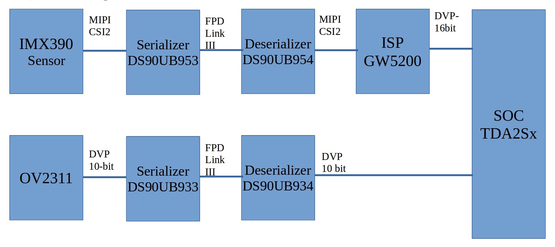
I am using TDA2Sx in my Custom board with 933 Ser - 934 Deser and 953 Ser - 954 Deser

Block Diagram :

OV2311 -> DS90UB933 <----STP------> DS90UB934 ---------> |  TDA2SX |

IMX390  -> DS90UB953 <----STP------> DS90UB954-->ISP-> |________|

What and all initialization sequence has to do follow ?

PDB, LOCK, PASS, OE configure as output and set to high for both Deserializers.

For CMLOUT (934) ->

  •     {0x01, 0x02},
  •     {0xb0, 0x04},
  •     {0xb1, 0x04},
  •     {0xb2, 0x1f},
  •     {0xb0, 0x04},
  •     {0xb1, 0x14},
  •     {0xb2, 0x1f},
  •     {0xb0, 0x08},
  •     {0xb1, 0x04},
  •     {0xb2, 0x1f},
  •     {0xb0, 0x08},
  •     {0xb1, 0x14},
  •     {0xb2, 0x1f},
  •     {0x41, 0xb6},
  •     {0x42, 0x75},
  •     {0x4c, 0x03},
  •     {0xd2, 0x9c},
  •     {0xb0, 0x05},
  •     {0xb1, 0x03},
  •     {0xb2, 0x06},
  •     {0xb1, 0x04},
  •     {0xb2, 0x06}, 
  •     {0x02, 0x9e},   
  •     {0x6D, 0x07},
  •     {0x58, 0x58}

then assigning serializer, senor ID and Alias ID address.

For CMLOUT (954) ->

  • reset
  • {0xB0,0x14},
  • {0xB1,0x00},
  • {0xB2,0x80},
  • {0xB1,0x03},
  • {0xB2,0x28},
  • {0xB1,0x04},
  • {0xB2,0x28},
  • {0xB1,0x02},
  • {0xB2,0x20},
  • {0xB0,0x04},
  • {0xB1,0x0F},
  • {0xB2,0x01},
  • {0xB1,0x10},
  • {0xB2,0x02},
  • {0x02, 0x9e},   
  • {0x6D, 0x07},
  • {0x58, 0x58}

Is this sequence registers are right ? Do I miss any information?

Regards,

ARUNKUMAR V N

  • Hi,

    Can anyone help me on this,

    i am waiting for response

    Regards,

    ARUNKUMAR V N

  • Hi Arunkumar,

    Is the IMX390 camera from D3? 

    This is because this camera board is already supported in the vision sdk, you could get the configuration for 953/960 from vision sdk.

    Regards,

    Brijesh

  • Hi Brijesh,

    Thanks for quick response,

     Actually, It's not for D3. It's for our Custom Board. The connection is like this.

    Even I referred D3 configuration also. But I am asking I2C sequence and all other initialization for our custom board.

    Whatever i mentioned the sequence registers above are right ? Do I miss any information?

    Regards,

    ARUNKUMAR V N

  • Hi,

    Can anyone help me on this,

    i am waiting for response

    Regards,

    ARUNKUMAR V N

  • Hi ArunKumar,

    D3 camera is what we support, for the new camera, it requires bringup.. Checking the sequence will not help much.

    Can you just try and see if it works.

    Rgds,

    Brijesh

  • Hi Brijesh,

    I tried like D3 Intialisation for my Camera. But in my custom board, we are not using IO Expander. I directly used GPIO to control all pins.

    These are the steps i did :

    1) Set PDB bits high for all FPD Link channels

    2) Set Lock and Pass bits high for Driver cam FPD Link channels

    3) Set OE bits high for all FPD Link channels

    But I missed other 2 steps :

    1) How to Enable VDD_FPD Sepic A, B - EN ? ( We are not using Sepic) ?

    2) How to Enable VDD_FPD Sepic Enable output power FPDA & B SW EN  ?

    which pins i have to enable ??


    Regards,

    ARUNKUMAR

  • Hi Arunkumar,

    Please check schematic of the board and set the pins accordingly.

    Rgds,

    Brijesh

  • Hi Brijesh,

    As per the schematic, i set the pins as like D3. These are the below pins configured in my custom board,

    • FPD_PDB
    • FPD_LOCK
    • FPD_PASS
    • FPD_OEn

    Anyhow in D3,  above pins and these below pins also enabled.

    /*Select voltage and Sepic A, B - 12V Sel*/
       if (voltage == BOARD_FPD_VOLTAGE_12V)
        {
            Bsp_boardSetBitsInGPIOExpander(KTCA9539_U33_I2CBUS, KTCA9539_U33_I2CADDR,
                                           BOARD_TCA9539_OUTPUT0_REG, 0x11);
        }*/

        /* Enable VDD_FPD Sepic A, B - EN */
        /*Bsp_boardSetBitsInGPIOExpander(KTCA9539_U33_I2CBUS, KTCA9539_U33_I2CADDR,
                                       BOARD_TCA9539_OUTPUT0_REG, 0x22);*/

        /* Enable output power FPDA & B SW EN */
        /*Bsp_boardSetBitsInGPIOExpander(KTCA9539_U33_I2CBUS, KTCA9539_U33_I2CADDR,
                                       BOARD_TCA9539_OUTPUT0_REG, 0x44);*/

    For my custom board,

    i am not using sepic chip. The VDD and VCC pins not configured as GPIO. Its handled in HW.

    So, My Question is :

    1) In 934 & 954 Deserializer what are the pins have to do pin muxing ?

    2) Is selecting FPD_Voltage from S/w side is neccessary ?

    Regards,

    ARUNKUMAR

  • Hi all,

    Can anyone help me on this,

    i am waiting for response

    1) What are the initialization sequence has to follow ?

    PDB, LOCK, PASS, OE configure as output and set to high for both De-serializers.

    2) I want to know the CMLOUT sequence for  934-933 and 954-953 De-serializer.

    Am I did proper sequence as like above mentioned in the post ? Any changes needed ?

    Regards,

    ARUNKUMAR V N

  • Hi,

    Can anyone response

    I am waiting for reply

    Regards,

    ARUNKUMAR

  • Hi Arun,

    I think you have started a new thread on this topic, so closing this thread.

    Rgds,

    Brijesh