Other Parts Discussed in Thread: TPS659037
I am evaluating the board for SITARA's USB 2.0 port.
In our USB2.0 circuit configuratio SITARA acts as a host.
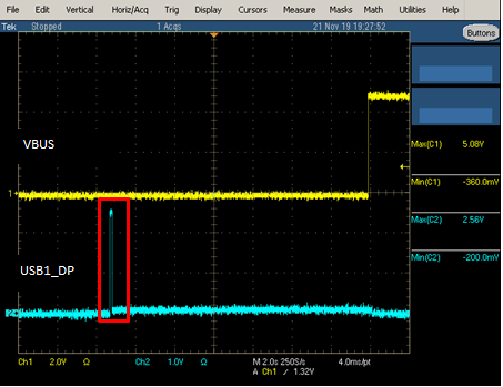
We turned on the board without connecting a USB device to the “USB1 port”.
And the waveform from “USB1_DP” to VBUS release was acquired.
And the waveform from “USB1_DP” to VBUS release was acquired.
Only on the USB1_DP side, a phenomenon of rising about 2.5 [V] occurred.(See waveform below)
This phenomenon occurred when power was supplied to the “VDDA33V_USB1” pin of SITARA from the power supply control IC (TPS6590377ZWST).
In addition, SITARA has confirmed that it is in a power-on reset state.
【QUESTION1】
What is the reason why only USB1_DP is excited about 2.5 [V]?
Is it affected by HI-Z? Or is the internal pull-up affected?
Does this always occur when using SITARA on the host? . If there is a way to avoid it, please let me know.
【QUESTION2】
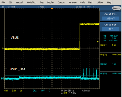
After canceling the power-on reset of SITARA,The USB_DP signal has changed to about 0 [V].
Is that because the USB 2.0 standard 15KΩ pull-down has been enabled?