This thread has been locked.

If you have a related question, please click the "Ask a related question" button in the top right corner. The newly created question will be automatically linked to this question.

AM3351: DDR2 DQS and DQ signal issue

Part Number: AM3351

Hi,

I previously posted questions about DDR2 measurements which were not okay. We have updated the design to solve the non conformance's. Now I do still see some strange behavior in our signals and was wondering if this is normal behavior or maybe a board or setting problem. (We are running at 266 MHz).

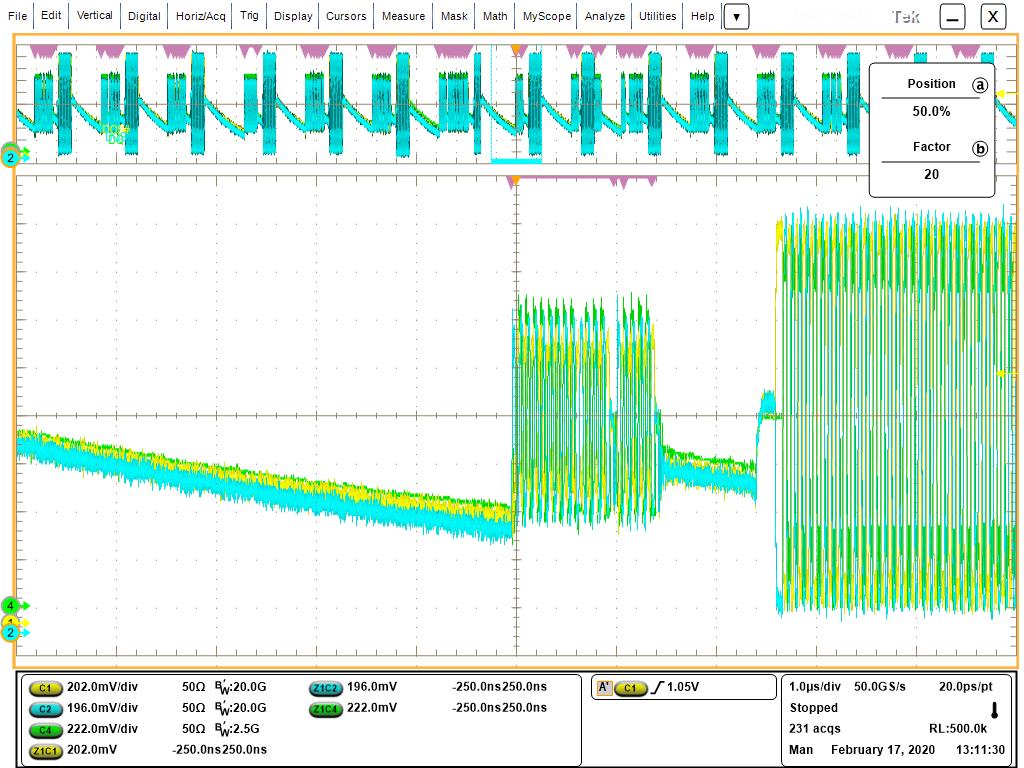
When writing to the memory the signals are looking like this:

and zoomed in:

The signals are measured at the DDR2 device:

S1 (Yellow) -> DQS1_n

S2 (Blue) -> DQS1_p

S4 (Green) -> DQ10

IO_CTRL_x = 0x0000030B

In the last picture where the DQS starts, a glitch or pulse is visible. Is this normal behavior of the signals? And can you give a statement about how the signals are looking?

Please let me know if you need more information. Thank you!

Regards,

F. Veger

  • Hi Francois, can you send the output file of the DSS script with your configuration, much like you did in the previous post?  This will give the full picture of how the controller and memory are configured.

    It may be that you need to adjust ODT on the memory, or there are still some layout anomalies resulting in what looks like signal reflection.  Can you also briefly describe the equpiment you are using to probe the signal 

    Do you see any functional issues?  Is the memory read/write access stable?

    Regards,

    James

  • Hi James,

    Yes hereby the output of the DSS file: 

    am335x-ddr-analysis_2020-02-21_131131.txt
    Switched to DAP_DebugSS
    Read value of 2b94402e from Device_ID register.
    CONTROL: device_id = 0x2b94402e
      * AM335x family
      * Silicon Revision 2.1
    
    CONTROL: control_status = 0x008c0356
      * SYSBOOT[15:14] = 10b (25 MHz)
    CM_CLKSEL_DPLL_DDR = 0x00010a18
      * DPLL_MULT = 266 (x266)
      * DPLL_DIV = 24 (/25)
    CM_DIV_M2_DPLL_DDR = 0x00000201
      * CLKST = 1: M2 output clock enabled
      * DIVHS = 1 (/1)
    
    DPLL_DDR Summary
     -> F_input = 25 MHz
     -> CLKOUT_M2 = DDR_PLL_CLKOUT = 266 MHz
    
    EMIF: SDRAM_CONFIG = 0x43845732
      * Bits 31:29 (reg_sdram_type) set for DDR2
      * Bits 28:27 (reg_ibank_pos) set to 0
      * Bits 26:24 (reg_ddr_term) set for 50 Ohm (011b)
      * Bit  23    (reg_ddr2_ddqs) set to differential DQS.
      * Bits 19:18 (reg_sdram_drive) set for weak drive (01b)
      * Bits 15:14 (reg_narrow_mode) set to 1 -> 16-bit EMIF interface
      * Bits 13:10 (reg_cl) set to 5 -> CL = 5
      * Bits 09:07 (reg_rowsize) set to 6 -> 15 row bits
      * Bits 06:04 (reg_ibank) set to 3 -> 8 banks
      * Bits 02:00 (reg_pagesize) set to 2 -> 10 column bits
    
    EMIF: PWR_MGMT_CTRL = 0x00000000
     * Bits 10:8 reg_lp_mode set to 0, auto power management disabled
     * Warning: Bits 7:4 (reg_sr_tim) are in violation of Maximum Self-Refresh Command Limit
       -> Please see the silicon errata (DDR3: JEDEC Compliance for Maximum Self-Refresh Command Limit) for more details.
       -> This is only an issue if used in conjunction with reg_lp_mode=2.
    
    DDR PHY: DDR_PHY_CTRL_1 = 0x00100306
      * Bits 9:8 (reg_phy_rd_local_odt) to 3 -> half thevenin termination
      * Bits 4:0 (reg_read_latency) set to 6
        -> If PHY_INVERT_CLKOUT=0, this is an appropriate value.
        -> If PHY_INVERT_CLKOUT=1, this is too small.
        -> PHY_INVERT_CLKOUT is a write-only register, so this needs to be
        -> inspected closely in the code and RatioSeed spreadsheet.
    
    *********************
    *** Register Dump ***
    *********************
    
    *(0x4c000000) = 0x40443403
    *(0x4c000004) = 0x40000004
    *(0x4c000008) = 0x43845732
    *(0x4c00000c) = 0x00000000
    *(0x4c000010) = 0x2000040d
    *(0x4c000014) = 0x0000040d
    *(0x4c000018) = 0x0666a392
    *(0x4c00001c) = 0x0666a392
    *(0x4c000020) = 0x142431ca
    *(0x4c000024) = 0x142431ca
    *(0x4c000028) = 0x0000021f
    *(0x4c00002c) = 0x0000021f
    *(0x4c000038) = 0x00000000
    *(0x4c00003c) = 0x00000000
    *(0x4c000054) = 0x00ffffff
    *(0x4c000058) = 0x8000140a
    *(0x4c00005c) = 0x00021616
    *(0x4c000080) = 0x008aa7fa
    *(0x4c000084) = 0x000cc7d0
    *(0x4c000088) = 0x00010000
    *(0x4c00008c) = 0x00000000
    *(0x4c000090) = 0x373bc7d8
    *(0x4c000098) = 0x00050000
    *(0x4c00009c) = 0x00050000
    *(0x4c0000a4) = 0x00000000
    *(0x4c0000ac) = 0x00000000
    *(0x4c0000b4) = 0x00000000
    *(0x4c0000bc) = 0x00000000
    *(0x4c0000c8) = 0x00000000
    *(0x4c0000d4) = 0x00000000
    *(0x4c0000d8) = 0x00000000
    *(0x4c0000dc) = 0x00000000
    *(0x4c0000e4) = 0x00100306
    *(0x4c0000e8) = 0x00100306
    *(0x4c000100) = 0x00000000
    *(0x4c000104) = 0x00000000
    *(0x4c000108) = 0x00000000
    *(0x4c000120) = 0x00000305
    
    ************************
    *** IOCTRL Registers ***
    ************************
    
    CONTROL: DDR_CMD0_IOCTRL = 0x0000030b
      * ddr_ba2 Pullup/Pulldown disabled
      * ddr_wen Pullup/Pulldown disabled
      * ddr_ba0 Pullup/Pulldown disabled
      * ddr_a5 Pullup/Pulldown disabled
      * ddr_ck Pullup/Pulldown disabled
      * ddr_ckn Pullup/Pulldown disabled
      * ddr_a3 Pullup/Pulldown disabled
      * ddr_a4 Pullup/Pulldown disabled
      * ddr_a8 Pullup/Pulldown disabled
      * ddr_a9 Pullup/Pulldown disabled
      * ddr_a6 Pullup/Pulldown disabled
      * Bits 9:5 control ddr_ck and ddr_ckn
        - Slew slowest
        - Drive Strength 5 mA
      * Bits 4:0 control ddr_ba0, ddr_ba2, ddr_wen, ddr_a[9:8], ddr_a[6:3]
        - Slew slow
        - Drive Strength 8 mA
    CONTROL: DDR_CMD1_IOCTRL = 0x0000030b
      * ddr_a15 Pullup/Pulldown disabled
      * ddr_a2 Pullup/Pulldown disabled
      * ddr_a12 Pullup/Pulldown disabled
      * ddr_a7 Pullup/Pulldown disabled
      * ddr_ba1 Pullup/Pulldown disabled
      * ddr_a10 Pullup/Pulldown disabled
      * ddr_a0 Pullup/Pulldown disabled
      * ddr_a11 Pullup/Pulldown disabled
      * ddr_casn Pullup/Pulldown disabled
      * ddr_rasn Pullup/Pulldown disabled
      * Bits 4:0 control ddr_15, ddr_a[12:10], ddr_a7, ddr_a2, ddr_a0, ddr_ba1, ddr_casn, ddr_rasn
        - Slew slow
        - Drive Strength 8 mA
    CONTROL: DDR_CMD2_IOCTRL = 0x0000030b
      * ddr_cke Pullup/Pulldown disabled
      * ddr_resetn Pullup/Pulldown disabled
      * ddr_odt Pullup/Pulldown disabled
      * ddr_a14 Pullup/Pulldown disabled
      * ddr_a13 Pullup/Pulldown disabled
      * ddr_csn0 Pullup/Pulldown disabled
      * ddr_a1 Pullup/Pulldown disabled
      * Bits 4:0 control ddr_cke, ddr_resetn, ddr_odt, ddr_csn0, ddr_[a14:13], ddr_a1
        - Slew slow
        - Drive Strength 8 mA
    CONTROL: DDR_DATA0_IOCTRL = 0x0000030b
      * ddr_d8 Pullup/Pulldown disabled
      * ddr_d9 Pullup/Pulldown disabled
      * ddr_d10 Pullup/Pulldown disabled
      * ddr_d11 Pullup/Pulldown disabled
      * ddr_d12 Pullup/Pulldown disabled
      * ddr_d13 Pullup/Pulldown disabled
      * ddr_d14 Pullup/Pulldown disabled
      * ddr_d15 Pullup/Pulldown disabled
      * ddr_dqm1 Pullup/Pulldown disabled
      * ddr_dqs1 and ddr_dqsn1 Pullup/Pulldown disabled
      * Bits 9:5 control ddr_dqs1, ddr_dqsn1
        - Slew slowest
        - Drive Strength 5 mA
      * Bits 4:0 control ddr_d[15:8], ddr_dqm1
        - Slew slow
        - Drive Strength 8 mA
    CONTROL: DDR_DATA1_IOCTRL = 0x0000030b
      * ddr_d0 Pullup/Pulldown disabled
      * ddr_d1 Pullup/Pulldown disabled
      * ddr_d2 Pullup/Pulldown disabled
      * ddr_d3 Pullup/Pulldown disabled
      * ddr_d4 Pullup/Pulldown disabled
      * ddr_d5 Pullup/Pulldown disabled
      * ddr_d6 Pullup/Pulldown disabled
      * ddr_d7 Pullup/Pulldown disabled
      * ddr_dqm0 Pullup/Pulldown disabled
      * ddr_dqs0 and ddr_dqsn0 Pullup/Pulldown disabled
      * Bits 9:5 control ddr_dqs0, ddr_dqsn0
        - Slew slowest
        - Drive Strength 5 mA
      * Bits 4:0 control ddr_d[7:0], dqm0
        - Slew slow
        - Drive Strength 8 mA
    CONTROL: DDR_IO_CTRL = 0x00000000
      * Bit 31: DDR_RESETn controlled by EMIF.
      * Bit 28 (mddr_sel) configured for SSTL, i.e. DDR2/DDR3/DDR3L operation.
    CONTROL: VTP_CTRL = 0x00010167
      * VTP not disabled (expected in normal operation, but not DS0).
    CONTROL: VREF_CTRL = 0x00000000
      * VREF supplied externally (typical).
    CONTROL: DDR_CKE_CTRL = 0x00000001
      * CKE controlled by EMIF (normal/ungated operation).
    

    The stability of the platform looks good, no functional issues.

    The equipment which I use to measure DDR2 is as follows:

    Oscilloscope: MSO73304DX

    Probe: P7720 with a solder-down tip (P77STFLXA) for DQS1_p

    Probe: P7720 with a solder-down tip (P77STFLXA) for DQS1_n

    Probe: TAP2500 connected to DQ10

    Regards,

    François

  • Francois,

    the only adjustments you could make for a write are the controller's drive strength and the memory's ODT.  Based on the log file you sent of the configuration, you have the drive strength set to 8mA for data (bits 4:0 of DDR_DATAx_IOCTRL) and 5mA for DQS (bits 9:5).  I would try making them both 5mA

    On the memory side, you have ODT set for 50ohms (bits 26:24 in SDRAM_CONFIG).  I think this should be adequate, but it also requires that the ODT signal is properly connected, otherwise the memory ODT will not enable

    Regards,

    James

  • Hi James,

    When I set the drive-strenght to 5mA the first part does not change the pulse/glitch in the beginning. (I set the IOCTRL to 0x318). (Additionally I noticed the green signal was not deskewed with the other signals, which I corrected in the new measurement.)

    It more looks like some initialization getting the signals to a valid level? I double checked the ODT line but it seems to be okay (AM3351 pin G1 to DDR memory pin K9). Is this behavior never seen at Texas Instruments?

    Regards,

    François

  • Hi Francois, the bump you are seeing is during the preamble, where the signals are transitioning from tri-state to driven.  There is no signal integrity defined during the preamble stage.  As long as the signals are stable at the end of the preamble stage (the first differential transition), things should work fine.  

    Regards,

    James