This thread has been locked.

If you have a related question, please click the "Ask a related question" button in the top right corner. The newly created question will be automatically linked to this question.

TMS320C6657: Error loading code via JTAG

Part Number: TMS320C6657
Other Parts Discussed in Thread: LM10011

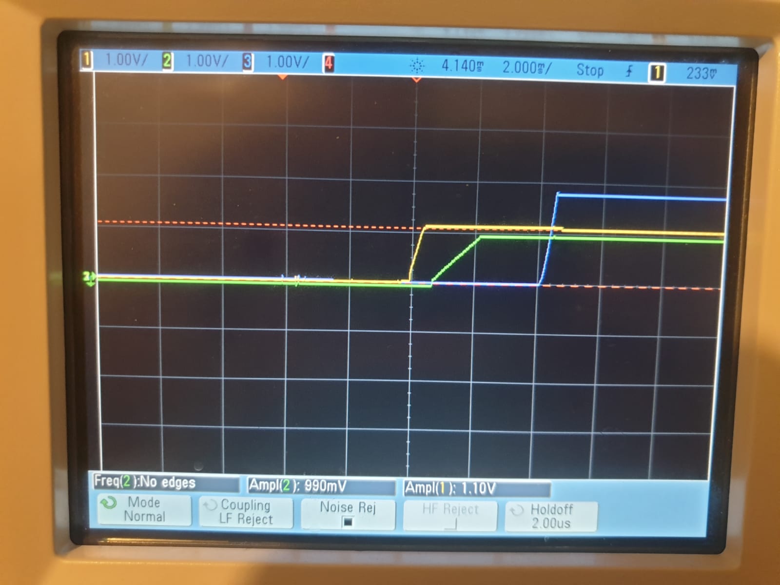
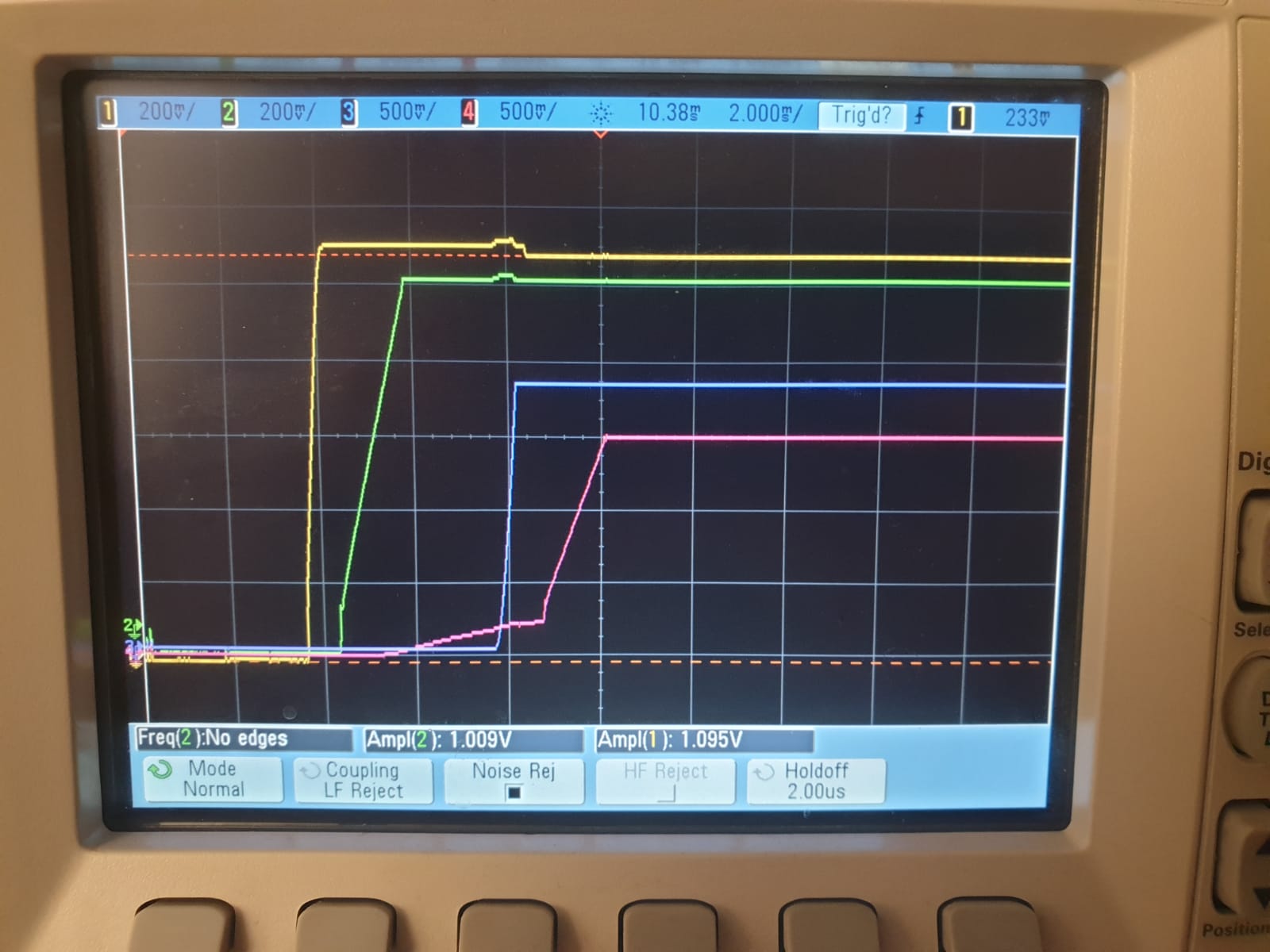
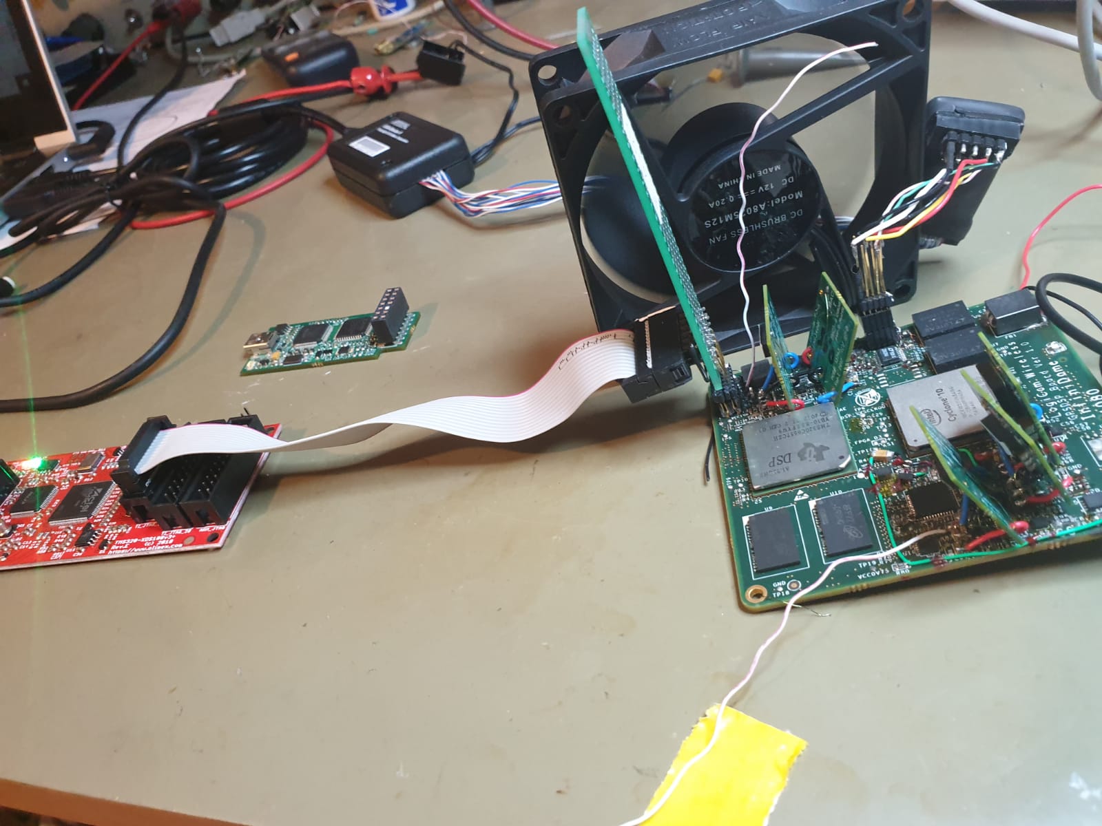
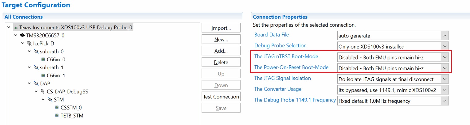
I have a custom board with C6657 and XDS100v2 JTAG emulator.

The "test connection" for the JTAG passes,

but when I try to connect to one of the cores - for core 1 i get the error:

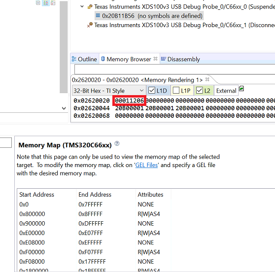
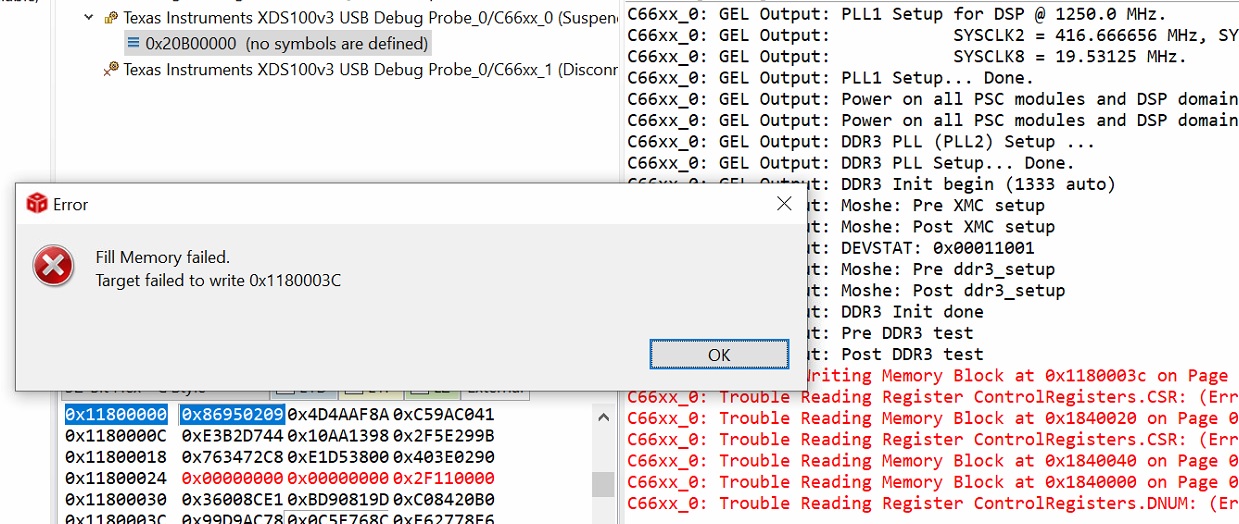
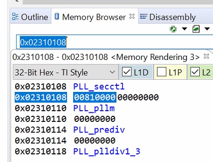
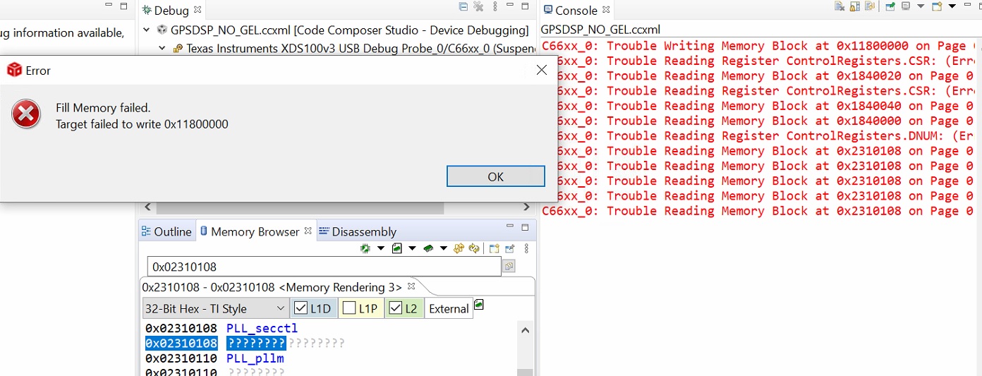
C66xx_1: Trouble Writing Memory Block at 0x800000 on Page 0 of Length 0x7ff0: (Error -1189 @ 0x800000) Requested operation failed for security violation. Check security/privilege settings, and retry the operation. (Emulation package 9.2.0.00002)
C66xx_1: File Loader: Verification failed: Target failed to write 0x00800000
C66xx_1: GEL: File: C:\ti\DSP_Tests Codes\test1.out: Load failed.

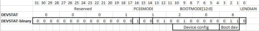
when i try to connect to core 0 - i get the error:

Error connecting to the target:
(Error -1143 @ 0x0)
Device core was hung. The debugger has forced the device to a ready state and recovered debug control, but your application's state is now corrupt. You should have limited access to memory and registers, but you may need to reset the device to debug further.
(Emulation package 9.2.0.00002)

C66xx_1: Power Failure on Target CPU
C66xx_1: Failed to remove the debug state from the target before disconnecting.  There may still be breakpoint op-codes embedded in program memory.  It is recommended that you reset the emulator before you connect and reload your program before you continue debugging
C66xx_0: Error connecting to the target: (Error -6306) Failed to connect to PRSC module. (Emulation package 9.2.0.00002)

Please advice what should i check.

Thanks,

Pavel

  • Hi, Pavel,

    Please see Debugging JTAG in the link below for the info on the error message.

    https://software-dl.ti.com/ccs/esd/documents/ccs_debugging_jtag_connectivity_issues.html

    Are the DSPs configured with GEL file?

    Rex

  • Hi,

    Please refer to the GEL file under CCS installation: ccs\ccs_base\emulation\boards\evmc6657l\gel\evmc6657l.gel. First connect to core 0 and let it run, the PLL and DDR3 settings may be different for your customized board, please update. Loading code into L2 should not be affected by DDR3 setting.

    Regards, Eric

  • Hi Eric, Thank you for your reply!

    Indeed, I use a GEL file (based on the one for the EVM but customized for my board). However, I have 2 issues:

    First, even before trying to load a code , I can't connect to core0 first. When I try to "connect to core 0", i get the error:

    "Error connecting to the target:
    (Error -1143 @ 0x0)
    Device core was hung. The debugger has forced the device to a ready state and recovered debug control, but your application's state is now corrupt. You should have limited access to memory and registers, but you may need to reset the device to debug further."

    I can however connect to core1, and after successfully connecting to core1 , i can connect to core0 despite getting an error.

    Second, I can't seem to be able to simply "write memory" even to L2 . After connecting to core1, in CCS i try to use "Tools -> Fill memory",
    I'm able to successfully write 32KB to 0x00e00000 (L1) , but once I try write even 100 bytes to 0x00800000 i get inconsistent behaviour:
    rarely i'm able to write , but most of the time i get an error:

    C66xx_1: Trouble Writing Memory Block at 0x800000 on Page 0 of Length 0xb4: (Error -1175 @ 0x800000) Requested operation failed for security violation. Check security/privilege settings, and retry the operation. (Emulation package 9.2.0.00002)

    after which I see only some of the data written (e.g. only first 80 bytes..)

    Appreciate your advice.

    Pavel

  • Hi Rex, thanks for your response!

    I went over the debugging JTAG connectivity, and it seems my connection is ok:

    [Start: Texas Instruments XDS100v2 USB Debug Probe_0]

    Execute the command:

    %ccs_base%/common/uscif/dbgjtag -f %boarddatafile% -rv -o -F inform,logfile=yes -S pathlength -S integrity

    [Result]


    -----[Print the board config pathname(s)]------------------------------------

    C:\Users\pavel\AppData\Local\TEXASI~1\CCS\
        ccs1000\0\0\BrdDat\testBoard.dat

    -----[Print the reset-command software log-file]-----------------------------

    This utility has selected a 100- or 510-class product.
    This utility will load the adapter 'jioserdesusb.dll'.
    The library build date was 'May  7 2020'.
    The library build time was '21:10:18'.
    The library package version is '9.2.0.00002'.
    The library component version is '35.35.0.0'.
    The controller does not use a programmable FPGA.
    The controller has a version number of '4' (0x00000004).
    The controller has an insertion length of '0' (0x00000000).
    This utility will attempt to reset the controller.
    This utility has successfully reset the controller.

    -----[Print the reset-command hardware log-file]-----------------------------

    The scan-path will be reset by toggling the JTAG TRST signal.
    The controller is the FTDI FT2232 with USB interface.
    The link from controller to target is direct (without cable).
    The software is configured for FTDI FT2232 features.
    The controller cannot monitor the value on the EMU[0] pin.
    The controller cannot monitor the value on the EMU[1] pin.
    The controller cannot control the timing on output pins.
    The controller cannot control the timing on input pins.
    The scan-path link-delay has been set to exactly '0' (0x0000).

    -----[The log-file for the JTAG TCLK output generated from the PLL]----------

    There is no hardware for programming the JTAG TCLK frequency.

    -----[Measure the source and frequency of the final JTAG TCLKR input]--------

    There is no hardware for measuring the JTAG TCLK frequency.

    -----[Perform the standard path-length test on the JTAG IR and DR]-----------

    This path-length test uses blocks of 64 32-bit words.

    The test for the JTAG IR instruction path-length succeeded.
    The JTAG IR instruction path-length is 6 bits.

    The test for the JTAG DR bypass path-length succeeded.
    The JTAG DR bypass path-length is 1 bits.

    -----[Perform the Integrity scan-test on the JTAG IR]------------------------

    This test will use blocks of 64 32-bit words.
    This test will be applied just once.

    Do a test using 0xFFFFFFFF.
    Scan tests: 1, skipped: 0, failed: 0
    Do a test using 0x00000000.
    Scan tests: 2, skipped: 0, failed: 0
    Do a test using 0xFE03E0E2.
    Scan tests: 3, skipped: 0, failed: 0
    Do a test using 0x01FC1F1D.
    Scan tests: 4, skipped: 0, failed: 0
    Do a test using 0x5533CCAA.
    Scan tests: 5, skipped: 0, failed: 0
    Do a test using 0xAACC3355.
    Scan tests: 6, skipped: 0, failed: 0
    All of the values were scanned correctly.

    The JTAG IR Integrity scan-test has succeeded.

    -----[Perform the Integrity scan-test on the JTAG DR]------------------------

    This test will use blocks of 64 32-bit words.
    This test will be applied just once.

    Do a test using 0xFFFFFFFF.
    Scan tests: 1, skipped: 0, failed: 0
    Do a test using 0x00000000.
    Scan tests: 2, skipped: 0, failed: 0
    Do a test using 0xFE03E0E2.
    Scan tests: 3, skipped: 0, failed: 0
    Do a test using 0x01FC1F1D.
    Scan tests: 4, skipped: 0, failed: 0
    Do a test using 0x5533CCAA.
    Scan tests: 5, skipped: 0, failed: 0
    Do a test using 0xAACC3355.
    Scan tests: 6, skipped: 0, failed: 0
    All of the values were scanned correctly.

    The JTAG DR Integrity scan-test has succeeded.

    [End: Texas Instruments XDS100v2 USB Debug Probe_0]

    One thing there that i'm not sure about is , it seems at first, it can't see the device, but later passes the scan-tests.

    Regarding GEL file, indeed i'm using GEL file to configure the DSP (right now something very basic, just PLLs and a few power domains not even DDR) but, I have 2 issues (even before trying to load a code).

    First, I can't connect to core0. When I try to "connect to core 0", i get the error:

    "Error connecting to the target:
    (Error -1143 @ 0x0)
    Device core was hung. The debugger has forced the device to a ready state and recovered debug control, but your application's state is now corrupt. You should have limited access to memory and registers, but you may need to reset the device to debug further."

    I can, however, connect to core1, and after successfully connecting to core1 , i can connect to core0 despite getting the same error again.

    Second, I can't seem to be able to simply "write memory" even to L2 . After connecting to core1, in CCS i try to use "Tools -> Fill memory",
    I'm able to successfully write 32KB to 0x00e00000 (L1) , but once I try write even 100 bytes to 0x00800000 i get inconsistent behaviour:
    rarely i'm able to write , but most of the time i get an error:

    C66xx_1: Trouble Writing Memory Block at 0x800000 on Page 0 of Length 0xb4: (Error -1175 @ 0x800000) Requested operation failed for security violation. Check security/privilege settings, and retry the operation. (Emulation package 9.2.0.00002)

    after which I see only some of the data written (e.g. only first 80 bytes..)

    Appreciate your advice.

    Pavel

  • Pavel,

    Thanks for the detailed post. Looking at the whole scenario, it seems the device itself is in an unstable state of sorts, since you are unable to connect to Core0 and Core1 local memory looks severely unstable. The exact root cause could be on the CCS (hardly), the Debug Probe (maybe) or the target board itself. I would start by replacing the target board with a well known working hardware (a C6678 EVM, for example) to try and isolate the issue to the board or the CCS+Debug Probe. 

    If the issue is detected on the CCS or Debug Probe, I would definitely go through the steps shown in the Troubleshooting section of the CCS User's Guide at:

    https://software-dl.ti.com/ccs/esd/documents/users_guide/index.html

    To troubleshoot the Debug Probe, check the reference sent by Rex above - pay special attention to the Hardware Checklist section, including items 7 and 8 that deal with ground loops and EMI/noise on the lines. I have seen pretty unstable connections be caused by these topics. Along the same lines, check your hardware and schematics against the XDS Target Connection Guide, which has implementation suggestions for the JTAG circuitry. 

    https://software-dl.ti.com/ccs/esd/documents/xdsdebugprobes/emu_xds_target_connection_guide.html

    From a pure JTAG standpoint, it is easy for an unstable power line or reset circuitry to fool the Debug Probe into thinking that either the connection is solid or the error is coming from somewhere else - in this case the core being hung due to a specific event or pre-loaded fimrware.

    Hope this helps,

    Rafael

  • Hi Rafael,

    I think i was able to cross the debug probe of my suspect list and pinpoint the errors i get to two cases:

    I'm now able to connect to both cores, but:

    from core1 , i'm able to write 1M of data using tools -> fill memory for both core1 and core0 L2 SRAM (writing to 1080 0000 and to 1180 0000)

    but from core0 , i'm able to write 1M of data only to 1080 0000, writing even single byte to 1180 0000 results in:

    C66xx_0: Trouble Reading Register ControlRegisters.CSR: (Error -1060 @ 0x41) Device is not responding to the request. Reset the device, and retry the operation. If error persists, confirm configuration, power-cycle the board, and/or try more reliable JTAG settings (e.g. lower TCLK). (Emulation package 9.2.0.00002)
    C66xx_0: Trouble Reading Register ControlRegisters.CSR: (Error -1060 @ 0x41) Device is not responding to the request. Reset the device, and retry the operation. If error persists, confirm configuration, power-cycle the board, and/or try more reliable JTAG settings (e.g. lower TCLK). (Emulation package 9.2.0.00002)
    C66xx_0: Trouble Reading Memory Block at 0x1840020 on Page 0 of Length 0x4: (Error -1060 @ 0x1840020) Device is not responding to the request. Reset the device, and retry the operation. If error persists, confirm configuration, power-cycle the board, and/or try more reliable JTAG settings (e.g. lower TCLK). (Emulation package 9.2.0.00002)
    C66xx_0: Trouble Reading Memory Block at 0x1840040 on Page 0 of Length 0x4: (Error -1060 @ 0x1840040) Device is not responding to the request. Reset the device, and retry the operation. If error persists, confirm configuration, power-cycle the board, and/or try more reliable JTAG settings (e.g. lower TCLK). (Emulation package 9.2.0.00002)
    C66xx_0: Trouble Reading Memory Block at 0x1840000 on Page 0 of Length 0x4: (Error -1060 @ 0x1840000) Device is not responding to the request. Reset the device, and retry the operation. If error persists, confirm configuration, power-cycle the board, and/or try more reliable JTAG settings (e.g. lower TCLK). (Emulation package 9.2.0.00002)
    C66xx_0: Trouble Reading Register ControlRegisters.DNUM: (Error -1060 @ 0x50) Device is not responding to the request. Reset the device, and retry the operation. If error persists, confirm configuration, power-cycle the board, and/or try more reliable JTAG settings (e.g. lower TCLK). (Emulation package 9.2.0.00002)

    The second issue i'm experiencing is , when in the GEL file i try to initialize the DDR related registers,

    C66xx_0: Trouble Writing Memory Block at 0x210000e4 on Page 0 of Length 0x4: (Error -1060 @ 0x210000E4) Device is not responding to the request. Reset the device, and retry the operation. If error persists, confirm configuration, power-cycle the board, and/or try more reliable JTAG settings (e.g. lower TCLK). (Emulation package 9.2.0.00002)
    C66xx_0: GEL: Error while executing OnTargetConnect(): Target failed to write 0x210000E4
         at (*((unsigned int *) (0x21000000+0x000000E4))&=~(0x00008000)) [init_testdsp.gel:197]
         at ddr3_setup_auto_lvl_1333(0) [init_testdsp.gel:485]
         at OnTargetConnect()
    C66xx_0: Trouble Reading Register ControlRegisters.CSR: (Error -1060 @ 0x41) Device is not responding to the request. Reset the device, and retry the operation. If error persists, confirm configuration, power-cycle the board, and/or try more reliable JTAG settings (e.g. lower TCLK). (Emulation package 9.2.0.00002)
    C66xx_0: Trouble Reading Register ControlRegisters.CSR: (Error -1060 @ 0x41) Device is not responding to the request. Reset the device, and retry the operation. If error persists, confirm configuration, power-cycle the board, and/or try more reliable JTAG settings (e.g. lower TCLK). (Emulation package 9.2.0.00002)
    C66xx_0: Trouble Reading Register ControlRegisters.CSR: (Error -1060 @ 0x41) Device is not responding to the request. Reset the device, and retry the operation. If error persists, confirm configuration, power-cycle the board, and/or try more reliable JTAG settings (e.g. lower TCLK). (Emulation package 9.2.0.00002)
    C66xx_0: Trouble Reading Memory Block at 0x1840020 on Page 0 of Length 0x4: (Error -1060 @ 0x1840020) Device is not responding to the request. Reset the device, and retry the operation. If error persists, confirm configuration, power-cycle the board, and/or try more reliable JTAG settings (e.g. lower TCLK). (Emulation package 9.2.0.00002)
    C66xx_0: Trouble Reading Memory Block at 0x1840040 on Page 0 of Length 0x4: (Error -1060 @ 0x1840040) Device is not responding to the request. Reset the device, and retry the operation. If error persists, confirm configuration, power-cycle the board, and/or try more reliable JTAG settings (e.g. lower TCLK). (Emulation package 9.2.0.00002)
    C66xx_0: Trouble Reading Memory Block at 0x1840000 on Page 0 of Length 0x4: (Error -1060 @ 0x1840000) Device is not responding to the request. Reset the device, and retry the operation. If error persists, confirm configuration, power-cycle the board, and/or try more reliable JTAG settings (e.g. lower TCLK). (Emulation package 9.2.0.00002)
    C66xx_0: Trouble Reading Register ControlRegisters.DNUM: (Error -1060 @ 0x50) Device is not responding to the request. Reset the device, and retry the operation. If error persists, confirm configuration, power-cycle the board, and/or try more reliable JTAG settings (e.g. lower TCLK). (Emulation package 9.2.0.00002)
    C66xx_0: Trouble Reading Memory Block at 0x2620018 on Page 0 of Length 0x4: (Error -1060 @ 0x2620018) Device is not responding to the request. Reset the device, and retry the operation. If error persists, confirm configuration, power-cycle the board, and/or try more reliable JTAG settings (e.g. lower TCLK). (Emulation package 9.2.0.00002)

    This happens when i do:

        //Do a PHY reset. Toggle DDR_PHY_CTRL_1 bit 15 0->1->0
        DDR_DDRPHYC &= ~(0x00008000);
        DDR_DDRPHYC |= (0x00008000);
        DDR_DDRPHYC &= ~(0x00008000);

    where

    #define DDR_BASE_ADDR          0x21000000
    #define DDR_DDRPHYC                 (*(unsigned int*)(DDR_BASE_ADDR + 0x000000E4))

    Any ideas?

    Thanks again,

    Pavel

  • Pavel,

    I found my C6657 board here and, as expected, it worked well with the GEL initialization scripts. 

    In your specific scenario, can you check the Registers and see if any MPU is configured or enabled? This could probably explain some of the memory access errors. This is usually disabled by default, but I wonder if the device bootmode could influence this (a device expert will have to confirm that). Another aspect is if there is code previously loaded to the board - I suspect not, but have to confirm.  

    From a hardware standpoint, I have seen such instability when one or more power lines of the DSP are unstable or noisy (these devices have multiple Vcore and Vio lines), especially due to the fact the internal memory and registers are failing to be written, not external DDR3. However, given you are resetting the DDR PHY, can you track the power supply and see if it sags during this process? That could explain why the debug probe is losing control over the device. 

    I suspect this is not your case, but I have to ask: you don't have any external watchdog timer or supervisor tied to the device, do you? This is not common on C66x boards (which you probably took the hardware design from), but that could also trigger all sorts of problems during board bringup. 

    I am reaching the end of my ideas on what may be going wrong with the board - obviously short of trying to de-solder/re-ball/re-solder the device.

    Hope this helps,

    Rafael

  • Pavel,

    Basic CCS emulator connectivity to the DSP only requires 3 things: power supplies ramped to their rated levels, proper clock inputs and removing the device from reset.  Please provide scope pictures showing that you meet the power sequencing requirements and that the voltages are the proper level.  You need to measure the supply voltages using robust probing methods near to the load to show supply stability and that you do not have excessive IR drop in the copper planes.  You should also show a capture of the CORECLK and you should measure the clock seen on SYSCLKOUT.

    What BOOTMODE are you using?  Can you read the DEVSTAT register to verify that the BOOTMODE was latched properly?  Note that if you are using the GPIO pins that are muxed for latching BOOTMODE, that you must be using logic with RESETSTATz to restore the BOOTMODE values to the pins whenever the pins can be latched.

    Tom

  • Hi Tom,

    the following HW test were done :

    1)      CVDD measured to be 1.1V (although setting to 1.0V probably since the addition of 0.1V by the on board SmartReflex circuit).

    2)      CVDD1 was 1.0V

    3)      VCC1V8 measured to be 1.8V.

    4)      The CoreclockP and N was 100MHz the DSP Sysclock output was measured as expected and we could able to set as required.

    Below a snapshot from a scope:

    (this is a measurement before capacitors to remove the DC)

    Coreclkout after succesfully setting the PLL (with GEL file):

    5)      The DDRclockP and N was measured and was as expected and we could able to set as required (started with 500MHz, 666MHz etc.

    6)      The DSP_RESETZ, DSP_PORZ, DSP_RESETFULLZ, DSP_LRESETNMIENZ signals were "H" level.

    7)      The power on sequence of CVDD, CVDD1, 1.8V, CoreClk and reset sequence was measured to be Ok.

    8)      All JTAG tests done by the XDS100 v3 were pass successfully.


    We will send a snapshot of power sequencing later today.


    The DSP and DDR3 supply pins and GND including the VDDT1, VDDT2, VDDR1, VDDR2 and all DDR3 supplies were connected as in the C6657 lite evm_sch_16-00132-02 schematics.


    At earlier stages the JTAG connection test did not pass, but after adding serial resistors on the TMS,TDI,TDO, TCK and RCK signals the XDS100 target test was pass successfully.

    (we tested with 2 emulators, XDS100v2 and XDS100v3)


    If any additional test or information as schematics for review are required then we can provide it.

    Can you suggest other  tests and measurement in HW in order to verify proper work of the HW?

    Is the JTAG target test successful pass means that the JTAG communication with the target DSP is reliable and can be trusted?


    With addition to the above please see  the following:


    I sent via Yaron  the PDF and DSN of the electrical schematics and the BRD files GPSDSP15_5  relates to the PCB version and GPSDSP2_001 relates to the board after corrections as cuts, jumpers and other changes.


    With addition,  I also did yesterday  detailed X ray test for all  DSP pins connections to the PCB, it was found to be Ok.

    we added, additional  missing  10nF values of capacitors (0201) , I were  connected then on the via close to the CVDD1 and GND pins of the DSP. with parallel to the assembled 100nF on two CVDD1 pins of the DSP I added 10nF capacitors.

    Currently there are CVDD1 pins of the DSP with 100nF others with 10nF or 1nF. Please see page25  in  the top- 1.0V.


    The devstat register value is:

    so the No-Boot bit is on. (emulation mode).

    Trying to setup the DDR using GEL file fails here:

      //Do a PHY reset. Toggle DDR_PHY_CTRL_1 bit 15 0->1->0
        DDR_DDRPHYC &= ~(0x00008000);
        DDR_DDRPHYC |= (0x00008000);
        DDR_DDRPHYC &= ~(0x00008000);

    where

    #define DDR_BASE_ADDR          0x21000000
    #define DDR_DDRPHYC                 (*(unsigned int*)(DDR_BASE_ADDR + 0x000000E4))

    I recieve the following errors:

    C66xx_0: Trouble Writing Memory Block at 0x210000e4 on Page 0 of Length 0x4: (Error -1060 @ 0x210000E4) Device is not responding to the request. Reset the device, and retry the operation. If error persists, confirm configuration, power-cycle the board, and/or try more reliable JTAG settings (e.g. lower TCLK). (Emulation package 9.2.0.00002)
    C66xx_0: GEL: Error while executing OnTargetConnect(): Target failed to write 0x210000E4
         at (*((unsigned int *) (0x21000000+0x000000E4))&=~(0x00008000)) [init_testdsp.gel:197]
         at ddr3_setup_auto_lvl_1333(0) [init_testdsp.gel:485]
         at OnTargetConnect()
    C66xx_0: Trouble Reading Register ControlRegisters.CSR: (Error -1060 @ 0x41) Device is not responding to the request. Reset the device, and retry the operation. If error persists, confirm configuration, power-cycle the board, and/or try more reliable JTAG settings (e.g. lower TCLK). (Emulation package 9.2.0.00002)
    C66xx_0: Trouble Reading Register ControlRegisters.CSR: (Error -1060 @ 0x41) Device is not responding to the request. Reset the device, and retry the operation. If error persists, confirm configuration, power-cycle the board, and/or try more reliable JTAG settings (e.g. lower TCLK). (Emulation package 9.2.0.00002)
    C66xx_0: Trouble Reading Register ControlRegisters.CSR: (Error -1060 @ 0x41) Device is not responding to the request. Reset the device, and retry the operation. If error persists, confirm configuration, power-cycle the board, and/or try more reliable JTAG settings (e.g. lower TCLK). (Emulation package 9.2.0.00002)
    C66xx_0: Trouble Reading Memory Block at 0x1840020 on Page 0 of Length 0x4: (Error -1060 @ 0x1840020) Device is not responding to the request. Reset the device, and retry the operation. If error persists, confirm configuration, power-cycle the board, and/or try more reliable JTAG settings (e.g. lower TCLK). (Emulation package 9.2.0.00002)
    C66xx_0: Trouble Reading Memory Block at 0x1840040 on Page 0 of Length 0x4: (Error -1060 @ 0x1840040) Device is not responding to the request. Reset the device, and retry the operation. If error persists, confirm configuration, power-cycle the board, and/or try more reliable JTAG settings (e.g. lower TCLK). (Emulation package 9.2.0.00002)
    C66xx_0: Trouble Reading Memory Block at 0x1840000 on Page 0 of Length 0x4: (Error -1060 @ 0x1840000) Device is not responding to the request. Reset the device, and retry the operation. If error persists, confirm configuration, power-cycle the board, and/or try more reliable JTAG settings (e.g. lower TCLK). (Emulation package 9.2.0.00002)
    C66xx_0: Trouble Reading Register ControlRegisters.DNUM: (Error -1060 @ 0x50) Device is not responding to the request. Reset the device, and retry the operation. If error persists, confirm configuration, power-cycle the board, and/or try more reliable JTAG settings (e.g. lower TCLK). (Emulation package 9.2.0.00002)
    C66xx_0: Trouble Reading Memory Block at 0x2620018 on Page 0 of Length 0x4: (Error -1060 @ 0x2620018) Device is not responding to the request. Reset the device, and retry the operation. If error persists, confirm configuration, power-cycle the board, and/or try more reliable JTAG settings (e.g. lower TCLK). (Emulation package 9.2.0.00002)

    Re/ memory fill from Core0 , we found the following:

    while writing 1Mbytes by  core0 of 0xFF to memory address 0x011800000 , the core crashes (with the errors from previous posts)

    After running Reset system and Reset emulator  commands using the CCS10 , Core0 recovers and reading this memory space shows bit errors in part of the memory address spaces.

    for example: in  start address 0x11800000 , instead written data as 0xFFFFFF there are addresses in that space that data is  read as  0xFFFFEF,  0xFFFFDF etc. That means that there are cases that one bit in the written word in many addresses is written as 0 instead of 1.

    The mistakes may be found in different bits bit of the data in  the word but only one bit for each data word in part of the words.

    Another thing we experience:

    Core1 write and read are done properly to address 0x11800000 and address 0x10800000 1M each.

    Core0 write and read are done properly to address 0x10800000 but as said, write to  address space start at 0x11800000 is not done properly and one of the bit in part of the words is written as 0 instead of 1.

    I tried to write manually to the behalf of Core0 to 0x11800000  8   bytes as 0x00 and it was written and read properly,

    but when tried to write again manually even to the same addresses the 8 bytes , it would crash we the above mentioned errors.

    After recovering of the CCS10,

     I tried to write manually  behalf of Core0 to 0x11800000  8   bytes as 0x00 and it was written and read properly.

    I did system reset by the CCS10 to Core0 and then I could right another 8 bytes to other address in the 1M address space started  at 0x11800000 properly and so on I could write properly after always  System reset each after the 8 bytes (or less) but only to addresses.

    but when I tried to write 9 bytes  or even 8 bytes spread ed on more then 2 sequential addresses  as 0x11800000, 0x11800004, 0x11800008 this would fail.

    The 8 bytes could be written properly only if it was started on addresses as 0x11800000, 0x11800004 or   0x11800004, 0x11800008 etc'

    Appreciate you adivce,

    Moshe & Pavel

  • The power sequence - scope screenshot -
    Yellow - CVDD

    Green - CVDD1

    Blue - VCC1V8 - 1.8V

  • Pavel,

    Can you show the power sequence including the DDR supply, DVDD15?  Can you show them with enough resolution to be able to measure the voltage levels?

    Tom

  • Moshe & Pavel,

    I have a few follow-up questions:

    How many boards have you assembled and tested? Do they all behave in the same manner?

    1)     CVDD measured to be 1.1V (although setting to 1.0V probably since the addition of 0.1V by the on board SmartReflex circuit).

    TI: Why do you make this assertion? Is it at 1.1V prior to reset release and then the CVDD supply drops to 1.0V after the VCNTL pins toggle?

    4)     The CoreclockP and N was 100MHz the DSP Sysclock output was measured as expected and we could able to set as required. Coreclkout after succesfully setting the PLL (with GEL file):

    TI: What was the frequency of the clock signal seen on SYSCLKOUT pin? You said that this was after PLL programming. What is the expected CORECLK rate after PLL programming?

    5)     The DDRclockP and N was measured and was as expected and we could able to set as required (started with 500MHz, 666MHz etc.

    TI: DDRCLKP/N is the reference clock for the DDR PLL. It should not be 500MHz or 666MHz. Please double check this. The DDRCLKP/N reference clock should be between 40MHz and 312MHz and is normally set to 100MHz or 66.6MHz. The clock out of the DDR PHY, DDRCLKOUTP/N[0], should be 533MHz or 666MHz. What do you see on these pins?

    6)     The DSP_RESETZ, DSP_PORZ, DSP_RESETFULLZ, DSP_LRESETNMIENZ signals were "H" level.

    TI: Can you provide a scope capture showing the sequencing of these reset signals rising.

    We added, additional missing 10nF values of capacitors (0201), I were connected then on the via close to the CVDD1 and GND pins of the DSP. with parallel to the assembled 100nF on two CVDD1 pins of the DSP I added 10nF capacitors. Currently there are CVDD1 pins of the DSP with 100nF others with 10nF or 1nF.

    TI: Did you do this to more than one board? Did you see any difference after adding the additional capacitors?

    The devstat register value is:

    TI: I could not see this image. What was the value? Does it align with the value expected from the BOOTMODE pins?

    so the No-Boot bit is on. (emulation mode).

    Trying to setup the DDR using GEL file fails here:

    //Do a PHY reset. Toggle DDR_PHY_CTRL_1 bit 15 0->1->0

       DDR_DDRPHYC &= ~(0x00008000);

       DDR_DDRPHYC |= (0x00008000);

       DDR_DDRPHYC &= ~(0x00008000);

    where

    #define DDR_BASE_ADDR          0x21000000

    #define DDR_DDRPHYC                 (*(unsigned int*)(DDR_BASE_ADDR + 0x000000E4))

    I recieve the following errors:

    C66xx_0: Trouble Writing Memory Block at 0x210000e4 on Page 0 of Length 0x4: (Error -1060 @ 0x210000E4) Device is not responding to the request. Reset the device, and retry the operation. If error

    Etc…

    TI: Those are basically READ-MODIFY-WRITE instructions to an internal register. The emulation error indicates that either the read or the write over JTAG failed. You need to get other basic JTAG operation robust before you proceed to DDR initialization.

    TI: Have you used CCS and an emulator with a C6657 EVM? It would be useful for you to operate with an EVM so that you can see how the emulator and the DSP should behave.

    Tom

  • Hi Tom, thanks for your thorough and detailed response!

    Below our answers to your questions:

    Tom: Can you show the power sequence including the DDR supply, DVDD15?  Can you show them with enough resolution to be able to measure the voltage levels?

    Moshe&Pavel:

    Yellow - CVDD - ~1.1V

    Green - CVDD1 - ~1V

    Blue - VCC1V8 - ~1.8V

    Pink - 1.5V to DDR3 - ~1.5V

    Tom: How many boards have you assembled and tested? Do they all behave in the same manner?

    M&P: We have assembled 2 boards. They don't behave in the same manner - all we wrote is regarding board #1.

    in board #2: we are only able to pass the JTAG connection test, but we are unable to connect to any of the cores. We think it might be an FPGA problem there (since we tried replacing the DSP).

    1)     CVDD measured to be 1.1V (although setting to 1.0V probably since the addition of 0.1V by the on board SmartReflex circuit).

    TI: Why do you make this assertion? Is it at 1.1V prior to reset release and then the CVDD supply drops to 1.0V after the VCNTL pins toggle?

    M&P: if we disconnect the dc2dc component , we measure 1.0V here, but once everything is connected we get 1.1V

    4)     The CoreclockP and N was 100MHz the DSP Sysclock output was measured as expected and we could able to set as required. Coreclkout after succesfully setting the PLL (with GEL file):

    TI: What was the frequency of the clock signal seen on SYSCLKOUT pin? You said that this was after PLL programming. What is the expected CORECLK rate after PLL programming?

    Pink - Sysclockout - ~160MHz

    Yellow - ResetZ

    Green - PORz

    Blue - ResetFullZ

    The coreclkP is ~100MHz, Sysclockout is ~160MHz (after GEL InitPLL , where we set PLL1 multiplier to 19 and PLL1 divider to 0, expecting 1000MHz (for the given 100MHz coreclk)).

    Before the InitPLL using GEL we get the following Sysclockout -

    here the Pink - sysclockout - is 250MHz (before GEL InitPLL).

    Yellow - ResetZ, Green - PORz, Blue - ResetFullZ.

    Note that the scope BW is 500MHz (hence ..)

    5)     The DDRclockP and N was measured and was as expected and we could able to set as required (started with 500MHz, 666MHz etc.

    TI: DDRCLKP/N is the reference clock for the DDR PLL. It should not be 500MHz or 666MHz. Please double check this. The DDRCLKP/N reference clock should be between 40MHz and 312MHz and is normally set to 100MHz or 66.6MHz. The clock out of the DDR PHY, DDRCLKOUTP/N[0], should be 533MHz or 666MHz. What do you see on these pins?

    M&P: Indeed, we previous wrote this wrong. The DDRCLKP is 50MHz.

    The DDRClkOut we were able to set to 500MHz and to 666MHz (different settings in InitPll2 in the GEL file, we were able to see this signal changing according to the values set in the GEL file).

    6)     The DSP_RESETZ, DSP_PORZ, DSP_RESETFULLZ, DSP_LRESETNMIENZ signals were "H" level.

    TI: Can you provide a scope capture showing the sequencing of these reset signals rising.

    M&P:

    Yellow - ResetZ

    Green - PORz

    Blue - ResetFullZ

    Here are 2 additional scope snapshots of CoreClkP (Pink) and ResetZ (Yellow):

    We added, additional missing 10nF values of capacitors (0201), I were connected then on the via close to the CVDD1 and GND pins of the DSP. with parallel to the assembled 100nF on two CVDD1 pins of the DSP I added 10nF capacitors. Currently there are CVDD1 pins of the DSP with 100nF others with 10nF or 1nF.

    TI: Did you do this to more than one board? Did you see any difference after adding the additional capacitors?

    M&P: only to the board we were able to connect to the cores. No difference.

    The devstat register value is:

    TI: I could not see this image. What was the value? Does it align with the value expected from the BOOTMODE pins?

    M&P:

    The value of the DEVSTAT register is 0x00011206, which set the boot device bits to NAND (this is not what we planned, and indeed we need to correct this) however, I'm not sure how this should related to the behaviour we describe.

    so the No-Boot bit is on. (emulation mode).

    Trying to setup the DDR using GEL file fails here:

    //Do a PHY reset. Toggle DDR_PHY_CTRL_1 bit 15 0->1->0

       DDR_DDRPHYC &= ~(0x00008000);

       DDR_DDRPHYC |= (0x00008000);

       DDR_DDRPHYC &= ~(0x00008000);

    where

    #define DDR_BASE_ADDR          0x21000000

    #define DDR_DDRPHYC                 (*(unsigned int*)(DDR_BASE_ADDR + 0x000000E4))

    I recieve the following errors:

    C66xx_0: Trouble Writing Memory Block at 0x210000e4 on Page 0 of Length 0x4: (Error -1060 @ 0x210000E4) Device is not responding to the request. Reset the device, and retry the operation. If error

    Etc…

    TI: Those are basically READ-MODIFY-WRITE instructions to an internal register. The emulation error indicates that either the read or the write over JTAG failed. You need to get other basic JTAG operation robust before you proceed to DDR initialization.

    M&P: We agree, we just mention this as another example of the behaviour we are trying to debug: 1. failure to write core1 L2 SRAM from core0, while able to write both core0 and core1 L2 SRAM from core1. and 2. failure to write DDRPHY register.

    TI: Have you used CCS and an emulator with a C6657 EVM? It would be useful for you to operate with an EVM so that you can see how the emulator and the DSP should behave.

    M&P: Yes, we have a C6657 evm, and we were able to perform those operations using the original evm GEL file and CCS.

    Your help is very much appreciated,

    Moshe & Pavel.

  • Moshe and Pavel,

    The power sequence and voltages look good in the scope capture. The reset and clock sequencing also looks good. You stated that you only have one partially working board and a second board under debug. Are any other boards being assembled or are you limited to these 2 for now?

    1)     CVDD measured to be 1.1V (although setting to 1.0V probably since the addition of 0.1V by the on board SmartReflex circuit).

    TI: Why do you make this assertion? Is it at 1.1V prior to reset release and then the CVDD supply drops to 1.0V after the VCNTL pins toggle?

    M&P: if we disconnect the dc2dc component , we measure 1.0V here, but once everything is connected we get 1.1V

    TI: I do not understand this answer. What is the dc2dc component? The power supply should generate 1.1V by default. You can prove this by disabling the LM10011 using the EN pin. Be sure to monitor the device’s temperature as it might heat up quickly when SmartReflex is disabled and you may need to supply additional cooling.

    4)     The CoreclockP and N was 100MHz the DSP Sysclock output was measured as expected and we could able to set as required. Coreclkout after succesfully setting the PLL (with GEL file):

    TI: What was the frequency of the clock signal seen on SYSCLKOUT pin? You said that this was after PLL programming. What is the expected CORECLK rate after PLL programming?

    The coreclkP is ~100MHz, Sysclockout is ~160MHz (after GEL InitPLL , where we set PLL1 multiplier to 19 and PLL1 divider to 0, expecting 1000MHz (for the given 100MHz coreclk)).

    Before the InitPLL using GEL we get the following Sysclockout -

    TI: SYSCLKOUT is CORECLK/6 so if the internal PLL is generating 1000MHz than the SYSCLKOUT pin will have 166MHz as you have observed.

    Before the InitPLL using GEL we get the following Sysclockout -

    here the Pink - sysclockout - is 250MHz (before GEL InitPLL).

    TI: Please double check this. When the PLL is in BYPASS, the SYSCLKOUT will be 16.6MHz assuming the reference clock input is 100MHz. If this output is truly 250MHz, that is a significant problem as the PLL is generating a clock much too fast and the results could be bad – both device overheating and the internal logic completely corrupted.


    The value of the DEVSTAT register is 0x00011206, which set the boot device bits to NAND (this is not what we planned, and indeed we need to correct this) however, I'm not sure how this should related to the behavior we describe.

    TI: I recommend that you focus on getting this value latched as intended. Latching an improper boot mode may cause the device to operate erratically and results are not defined. DSP cores that are not in a stable state often fail to connect from CCS. This may also explain the improper PLL setting discussed earlier.

    Tom

  • Hi Tom,

    TI: I do not understand this answer. What is the dc2dc component? The power supply should generate 1.1V by default. You can prove this by disabling the LM10011 using the EN pin. Be sure to monitor the device’s temperature as it might heat up quickly when SmartReflex is disabled and you may need to supply additional cooling.

    The CVDD is provided on board by TI LM21215A-1 DCDC convertor.

    The RFB1 is 6.81 Kohm and RFB2 is 8.25 Kohm

     From the datasheet (see below)  the Vout (CVDD) is calculated to be  1.095V  per these RFB resistors so that is the Voltage that is actually  measured on CVDD.

    The CVDD is stable before and after RESET signals released  so you can currently  ignore the said about the SmartReflex activation.

     If necessary I can replace RFB1 to 4 Kohm and RFB2 to 10 Kohm in order to provide CVDD to be  1.0V.

    schematics of the CVDD DCDC and the SmartReflex on board circuits:

    TI: Please double check this. When the PLL is in BYPASS, the SYSCLKOUT will be 16.6MHz assuming the reference clock input is 100MHz. If this output is truly 250MHz, that is a significant problem as the PLL is generating a clock much too fast and the results could be bad – both device overheating and the internal logic completely corrupted.


    So , i have a "theory" why the 250MHz,

    Since, before GEL pll init, for some reason when I connect to the DSP without GEL initialization i see the value of 0x00090000 for SECCTL register:

    so if the BYPASS bit is 0, the DSP uses BOOTMODE pins for setting the PLLM and PLLD:

    since we had the DEVSTAT value of:

    for the 1250MHz chip and CLKIN of 100MHz, with 0b010 for BOOTMODE[12:10] we get:

    CLK = 100MHz * (16) = 1600MHz

    and then SYSCLKOUT = CLK / 6 = 266.66 MHz (which is about what we measured).

    I don't have an explanation for why the bypass bit in SECCTL was off after power on reset. It supposed to be off:

    "For power-onreset,the MainPLL Controllercomesup in bypassmodeand thePLL is not enabled" according to the datasheet.

    TI: I recommend that you focus on getting this value latched as intended. Latching an improper boot mode may cause the device to operate erratically and results are not defined. DSP cores that are not in a stable state often fail to connect from CCS. This may also explain the improper PLL setting discussed earlier.


    We latched the values for BOOTMODE[2:0] to 0b000 = No boot.

    Now, indeed before GEL Pll init, the sysclkout is 16.66MHz (100MHz (clkin) / 6).

    And now we are able to do fill memory of 52 bytes from core0 to 0x11800000 (before that we could only do 8 bytes, so that's some progress :-p)

    Any ideas?

    Thanks,

    Moshe & Pavel

  • Moshe and Pavel,

    I recommend that you work to have a start-up sequence where a proper BOOTMODE is latched and where the PLL only operates within the devices ratings.  These need to occur repeatedly and robustly.  Then you can trust your results.  You also need to have one or more additional boards for comparison.

    Tom

  • Tom,

    We succeeded to activate the other problematic board, where we could not connect to the DSP Cores before  (after replacement of a defected PD resistor of  the RESETz signal that is provided by the FPGA)


    We received the same behavior and results as received with the first board that we tested. The behavior we describe is consistent across both boards and systems.


    Core0 in both boards can still write only 52 bytes to address starts at 0X11800000 or to any other address in the same 1M memory block.

    If more than 52 bytes are written then the CCS10 crashes (with the errors above) and we need to reset several times the system, disconnect the cores and several  system reset and reconnect the cores.


    The other 1M memory block starting at 0X10800000 ,  can be  written and read properly by both cores.

    Another thing, for example, that causes such a crash, is an attempt to set DDRPHY register by core0 (by GEL file).

     We hope that the same received results  may give a better direction for solving the memory and registers access  problems as described.

    Moshe & Pavel.

  • Pavel, thank you for verifying all of the above and since your boot mode is now being set properly, you should check your device symbol against the data sheet to see if there are any differences.  There might be a ball connected incorrectly.  Also, compare your board to the EVM to see if there is a difference, maybe something is tied off wrong.  

  • Jeff,


    Since the instability of reading and writing several registers by the C6657 Core0, I'm still thinking about possible powering issues:


    1)      The CVDD voltage may be step out of limitation, measured to be  1.095V after rest sequence. Is that value is Ok or may be need to be reduced as to to 1.0V?

    2)      Since most of the access to memory and register problems are with  Core0, do you have any documentation or information regarding the CVDD pinout and the pin list  that are referred and supply the voltage  to Core0 and the other CVDD supply pins  that are referred and supply the voltage  to Core1? If you can provide  that information, can you send it?


    We still get unstable and inconsistent behavior on core0, e.g. , failure to connect to the core / we were able to setup DDR (and check read/write) using GEL file (but only once, further attempts failed) / failure to try and read control register (from 0x0262yyyy) after being able to successfully read them etc.)

    Re/ incorrectly connected ball - we did an x-ray test - and it all seemed well. Any idea which pin might cause such a behavior ?

    Thank you,

    Moshe & Pavel

  • Moshe & Pavel

    Reading through the entire thread - it is unclear how you have resolved the incorrect DEVSTAT latching and do you know for sure that for all your debug you are working with no boot/emulation boot mode, to ensure ROM is not impacting anything in terms of erratic behavior etc.

    Since power, clock , reset  looks reasonably ok, and it is access to on chip RAMs that seems to be not happening correctly can you doubly ensure that your CVDD and CVDD1 pins are correctly done on your board?

    Is it possible to run the device at a lower frequency and potentially with DDR not configured to see if the issues with core connectivity and memory access still persist?

    Regards

    Mukul

  • Mukul,

    Our DEVSTAT register to "no boot" using PD resistors on the relevant pins "BOOTMODE[2:0]".

    When we check the DEVSTAT register with memory browser at 0x02620020 the settings is as intended.

    If i suspend any execution on both cores, and not allowing any interrupts - how could ROM impact anything there?

    Re/ CVDD - we would like to reiterate our question-

    1) is 1.095V within the allowed range? (according to the datasheet p.37 it is)

    2) Since most of the access to memory and register problems are with  Core0, do you have any documentation or information regarding the CVDD pinout and the pin list  that are referred and supply the voltage  to Core0 and the other CVDD supply pins  that are referred and supply the voltage  to Core1? If you can provide  that information, can you send it?

    We don't do configure DDR in the GEL file, we just initialize the PLL for 1000MHz clock (with 1250MHz device), and configure L1 as cache and L2 as SRAM. that's it. nothing else.

    And still we are able to do fill memory to 0x10800000 and to 0x11800000 of 1M size from core1, but from core0 we are only able to fill memory to 0x10800000 but after writing 52 bytes to 0x11800000 we fail.

    (this is only one symptom, one that we are able to recreate consistently , other problem from core0 are less consistent).

    Any ideas would help.

    Pavel & Moshe

  • (follow up from Moshe)

    I rechecked all relevant  powering pins against the schematics against the pinout matrix as in the C6657  datasheet.

    The powering types were: CVDD, CVDD1, 1.8V, 1.5V, GND

    All pins refer the matrix were connected properly in the electrical schematics.


    I didn't find  any of the above checked types of powering pin in the matrix that was not connected.


    I attached the photo of the matrix where the marked pins are with different color for each supply type.

    The CVDD was marked with yellow, some of the CVDD pins were marked with circled color as well according to the bypass capacitor that was initially assembled on the PCB. About 7 missing bypass capacitors were assembled later manually on the PCB, I sent the scanning of the same matrix with the values and location pf the bypass capacitors on CVDD including the later added caps.


    Since the instability of reading and writing several to registers by the C6657 Core0, I'm still thinking about possible powering issues:


    1)    The CVDD voltage may be step out of limitation, measured to be  1.095V after rest sequence. Is that value is Ok or may be need to be reduced as to 1.0V?

    2)    Since most of the access to memory and register problems are with  Core0, do you have any documentation or information regarding the CVDD pinout and the pin list  that are referred and supply the voltage  to Core0 and the other CVDD supply pins  that are referred and supply the voltage  to Core1? If you can provide  that information, can you send it?


    Regards,

    Moshe

  • Hi Pavel

    >>If i suspend any execution on both cores, and not allowing any interrupts - how could ROM impact anything there?

    Ok. will assume that ROM is not in play in your current debug.

    >>1) is 1.095V within the allowed range? (according to the datasheet p.37 it is)

    Yes, assuming that you have understood the discussion with Tom around SR etc - 1.095 is within spec , and I don't see this as an area to focus for the current debug.

    2) Since most of the access to memory and register problems are with  Core0, do you have any documentation or information regarding the CVDD pinout and the pin list  that are referred and supply the voltage  to Core0 and the other CVDD supply pins  that are referred and supply the voltage  to Core1? If you can provide  that information, can you send it?


    I looked at the internal design specs, there is no further distinction specified on the power pins going to core 0 vs core 1 - the design is for the corepac - so no internal information that we can share on this to further help with your debug.

    >>And still we are able to do fill memory to 0x10800000 and to 0x11800000 of 1M size from core1, but from core0 we are only able to fill memory to 0x10800000 but after writing 52 bytes to 0x11800000 we fail.

    Is there failure only most reliably reproducible with the memory location you listed , what if you have a different start address etc? Is the error /crash message always the same?

  • Thanks Mukul,

    I rechecked the other DSP pinouts compatibility between the schematics, the datasheet ( matrix and tables) and the EVM schematics.

    The only found differences, were with the DSP  pins F22 and D23 that were connected in the EVM to PU 4.7K as well as in our target board while according  the data sheet they should be left unconnected.


    Before removing these two PUs,  can you understand why it was added  in the EVM (see the EVM schematics, page 18 – Smart Reflex)?

    Can you update us  if these PUs can be a reason to our R/W problems as we saw especially with  Core0?

    I rechecked all relevant  powering pins against the schematics against the pinout matrix as in the C6657  datasheet.

    The powering types were: CVDD, CVDD1, 1.8V, 1.5V, GND

    All pins refer the matrix were connected properly in the electrical schematics.


    I didn't find  any, of the above checked types, of powering pin in the matrix that was not connected.


    The CVDD was marked with yellow, some of the CVDD pins were marked with circled color as well according to the bypass capacitor that was initially assembled on the PCB. About 7 pins that were not directly connected to  bypass capacitors were assembled later manually on the PCB, I already sent the scanning of the same matrix with the values and location pf the bypass capacitors on CVDD including the later added caps.

    >> Is there failure only most reliably reproducible with the memory location you listed , what if you have a different start address etc? Is the error /crash message always the same?

    Additional consistently reproducible failure is the following:

    If, in the debug session, I'm disconnected from core1, at first attempt i can connect to core0, but if i disconnect

    and try to connect again, i get the failure ---

    Error connecting to the target:
    (Error -1143 @ 0x0)
    Device core was hung. The debugger has forced the device to a ready state and recovered debug control, but your application's state is now corrupt. You should have limited access to memory and registers, but you may need to reset the device to debug further.
    (Emulation package 9.2.0.00002)

    The interesting thing is, this doesn't happen when core1 is connected.

    After acknowledging the error, i'm able to connect to the core..

    An inconsistent error i sometime get when trying to connect is:

    Error connecting to the target:
    (Error -182 @ 0x0)
    The controller has detected a cable break that is near-to itself.
    The user must connect the cable/pod to the controller.
    (Emulation package 9.2.0.00002)

    Regarding the other consistent error:

    I'm able to do fill memory from core1 to 0x10800000 and 0x11800000 of size 1M (as many times as i like):

    BUT from core0 i'm able to fill memory to 0x10800000 of size 1M as many times as i wish BUT I can't write more than 52 bytes starting from any offset of 0x1180zzzz, and i can only do it once.

    second attempt of writing even 8 bytes even to the same address, results in:

    followed by:

    C66xx_0: Trouble Reading Register ControlRegisters.CSR: (Error -1060 @ 0x41) Device is not responding to the request. Reset the device, and retry the operation. If error persists, confirm configuration, power-cycle the board, and/or try more reliable JTAG settings (e.g. lower TCLK). (Emulation package 9.2.0.00002)
    C66xx_0: Trouble Reading Memory Block at 0x1840020 on Page 0 of Length 0x4: (Error -1060 @ 0x1840020) Device is not responding to the request. Reset the device, and retry the operation. If error persists, confirm configuration, power-cycle the board, and/or try more reliable JTAG settings (e.g. lower TCLK). (Emulation package 9.2.0.00002)
    C66xx_0: Trouble Reading Memory Block at 0x1840040 on Page 0 of Length 0x4: (Error -1060 @ 0x1840040) Device is not responding to the request. Reset the device, and retry the operation. If error persists, confirm configuration, power-cycle the board, and/or try more reliable JTAG settings (e.g. lower TCLK). (Emulation package 9.2.0.00002)
    C66xx_0: Trouble Reading Memory Block at 0x1840000 on Page 0 of Length 0x4: (Error -1060 @ 0x1840000) Device is not responding to the request. Reset the device, and retry the operation. If error persists, confirm configuration, power-cycle the board, and/or try more reliable JTAG settings (e.g. lower TCLK). (Emulation package 9.2.0.00002)
    C66xx_0: Trouble Reading Register ControlRegisters.CSR: (Error -1060 @ 0x41) Device is not responding to the request. Reset the device, and retry the operation. If error persists, confirm configuration, power-cycle the board, and/or try more reliable JTAG settings (e.g. lower TCLK). (Emulation package 9.2.0.00002)
    C66xx_0: Trouble Reading Register ControlRegisters.DNUM: (Error -1060 @ 0x50) Device is not responding to the request. Reset the device, and retry the operation. If error persists, confirm configuration, power-cycle the board, and/or try more reliable JTAG settings (e.g. lower TCLK). (Emulation package 9.2.0.00002)
    C66xx_0: Trouble Reading Memory Block at 0x11800400 on Page 0 of Length 0xa1: (Error -1060 @ 0x11800400) Device is not responding to the request. Reset the device, and retry the operation. If error persists, confirm configuration, power-cycle the board, and/or try more reliable JTAG settings (e.g. lower TCLK). (Emulation package 9.2.0.00002)
    C66xx_0: Trouble Reading Memory Block at 0x11800400 on Page 0 of Length 0xa1: (Error -1060 @ 0x11800400) Device is not responding to the request. Reset the device, and retry the operation. If error persists, confirm configuration, power-cycle the board, and/or try more reliable JTAG settings (e.g. lower TCLK). (Emulation package 9.2.0.00002)
    C66xx_0: Trouble Reading Memory Block at 0x11800400 on Page 0 of Length 0xa1: (Error -1060 @ 0x11800400) Device is not responding to the request. Reset the device, and retry the operation. If error persists, confirm configuration, power-cycle the board, and/or try more reliable JTAG settings (e.g. lower TCLK). (Emulation package 9.2.0.00002)
    C66xx_0: Trouble Reading Memory Block at 0x11800400 on Page 0 of Length 0xa1: (Error -1060 @ 0x11800400) Device is not responding to the request. Reset the device, and retry the operation. If error persists, confirm configuration, power-cycle the board, and/or try more reliable JTAG settings (e.g. lower TCLK). (Emulation package 9.2.0.00002)
    C66xx_0: Trouble Reading Memory Block at 0x11800400 on Page 0 of Length 0xa1: (Error -1060 @ 0x11800400) Device is not responding to the request. Reset the device, and retry the operation. If error persists, confirm configuration, power-cycle the board, and/or try more reliable JTAG settings (e.g. lower TCLK). (Emulation package 9.2.0.00002)

    Appreciate your help here..

    Moshe & Pavel

  • Hi 

    Thanks for additional details 

    1) On your query on the reserved pins. These pins are internally I2C like pins (open drain) that were intended for SR voltage control. This feature is not supported. I do not think these are the cause for the issue - you can see that the EVM is not impacted. However in your final design I would recommend adhering to the datasheet recommendations. 

    2) The error message images that you tried to embed are not visible - can you please share again?

    Additional questions/comments


    1] Connecting to core0 and receiving -1143 error

    a] The -1143 error indicates that the C66x is hung.  I know you are running these experiments in no boot mode - can you confirm if the code/ PC is in ROM or are you executing some code. Uninitialized code can cause code hangs.   After Connecting the core0 and receiving the -1143 error, what is the PC of the C66x?  Is the PC different from the first successful connection of core0? 

    b] Additionally it sounds like you are able to connect to core 0 the first time without error.  Is that always the case?  Typically in CCS you can have the configuration such that some device specific gel files can run on target connect - could it be that after gel fie/ target connect your user code is doing something to cause a crash? 

    2] "BUT from core0 i'm able to fill memory to 0x10800000 of size 1M as many times as i wish BUT I can't write more than 52 bytes starting from any offset of 0x1180zzzz, and i can only do it once."

    a] Is this the case during the first connect to core 0?  

      b] 0x11800000 is core1’s L2.  If core0 is having an issue accessing core1’s L2 but not its own then the C66x’s XMC might be in a bad state.  DO you see similar  read/write problems when trying to access DDR?


    3] The "inconsistent error" of -182 seems to imply an XDS probe error.  I know you are using XDS100v2, talking to emulation experts, we typically never see this message with XDS100v2- do you have other JTAG to try this with?

    4) I still did not see a confirmation on whether if you run in no boot mode, can you check if the crashes happen irrespective of whether the PLLs are in bypass mode (which i believe should be the case in no boot mode and no gel files run to configure PLLs to run at speed etc) vs running at speed?

    Regards

    Mukul 

  • Hi 

    >> 2) The error message images that you tried to embed are not visible - can you please share again?

    Here's an example of such error. This happened after i first tried to fill memory 10 bytes at 0x11800024 , following by trying to write 60 bytes to 0x1180003C.

    The console errors are:

    C66xx_0: Trouble Writing Memory Block at 0x1180003c on Page 0 of Length 0x3c: (Error -1060 @ 0x11800068) Device is not responding to the request. Reset the device, and retry the operation. If error persists, confirm configuration, power-cycle the board, and/or try more reliable JTAG settings (e.g. lower TCLK). (Emulation package 9.2.0.00002)
    C66xx_0: Trouble Reading Register ControlRegisters.CSR: (Error -1060 @ 0x41) Device is not responding to the request. Reset the device, and retry the operation. If error persists, confirm configuration, power-cycle the board, and/or try more reliable JTAG settings (e.g. lower TCLK). (Emulation package 9.2.0.00002)
    C66xx_0: Trouble Reading Memory Block at 0x1840020 on Page 0 of Length 0x4: (Error -1060 @ 0x1840020) Device is not responding to the request. Reset the device, and retry the operation. If error persists, confirm configuration, power-cycle the board, and/or try more reliable JTAG settings (e.g. lower TCLK). (Emulation package 9.2.0.00002)
    C66xx_0: Trouble Reading Register ControlRegisters.CSR: (Error -1060 @ 0x41) Device is not responding to the request. Reset the device, and retry the operation. If error persists, confirm configuration, power-cycle the board, and/or try more reliable JTAG settings (e.g. lower TCLK). (Emulation package 9.2.0.00002)
    C66xx_0: Trouble Reading Memory Block at 0x1840040 on Page 0 of Length 0x4: (Error -1060 @ 0x1840040) Device is not responding to the request. Reset the device, and retry the operation. If error persists, confirm configuration, power-cycle the board, and/or try more reliable JTAG settings (e.g. lower TCLK). (Emulation package 9.2.0.00002)
    C66xx_0: Trouble Reading Memory Block at 0x1840000 on Page 0 of Length 0x4: (Error -1060 @ 0x1840000) Device is not responding to the request. Reset the device, and retry the operation. If error persists, confirm configuration, power-cycle the board, and/or try more reliable JTAG settings (e.g. lower TCLK). (Emulation package 9.2.0.00002)
    C66xx_0: Trouble Reading Register ControlRegisters.DNUM: (Error -1060 @ 0x50) Device is not responding to the request. Reset the device, and retry the operation. If error persists, confirm configuration, power-cycle the board, and/or try more reliable JTAG settings (e.g. lower TCLK). (Emulation package 9.2.0.00002)
    C66xx_0: Trouble Reading Memory Block at 0x11800000 on Page 0 of Length 0x55: (Error -1060 @ 0x11800000) Device is not responding to the request. Reset the device, and retry the operation. If error persists, confirm configuration, power-cycle the board, and/or try more reliable JTAG settings (e.g. lower TCLK). (Emulation package 9.2.0.00002)
    C66xx_0: Trouble Reading Memory Block at 0x11800000 on Page 0 of Length 0x55: (Error -1060 @ 0x11800000) Device is not responding to the request. Reset the device, and retry the operation. If error persists, confirm configuration, power-cycle the board, and/or try more reliable JTAG settings (e.g. lower TCLK). (Emulation package 9.2.0.00002)
    C66xx_0: Trouble Reading Memory Block at 0x11800000 on Page 0 of Length 0x55: (Error -1060 @ 0x11800000) Device is not responding to the request. Reset the device, and retry the operation. If error persists, confirm configuration, power-cycle the board, and/or try more reliable JTAG settings (e.g. lower TCLK). (Emulation package 9.2.0.00002)
    C66xx_0: Trouble Reading Memory Block at 0x11800000 on Page 0 of Length 0x55: (Error -1060 @ 0x11800000) Device is not responding to the request. Reset the device, and retry the operation. If error persists, confirm configuration, power-cycle the board, and/or try more reliable JTAG settings (e.g. lower TCLK). (Emulation package 9.2.0.00002)
    C66xx_0: Trouble Reading Memory Block at 0x11800000 on Page 0 of Length 0x55: (Error -1060 @ 0x11800000) Device is not responding to the request. Reset the device, and retry the operation. If error persists, confirm configuration, power-cycle the board, and/or try more reliable JTAG settings (e.g. lower TCLK). (Emulation package 9.2.0.00002)

    >> Additional questions/comments


    >> 1] Connecting to core0 and receiving -1143 error

    >> a] The -1143 error indicates that the C66x is hung.  I know you are running these experiments in no boot mode - can you confirm if the code/ PC is in ROM or are you executing some code. Uninitialized code can cause code hangs.   After Connecting the core0 and receiving the -1143 error, what is the PC of the C66x?  Is the PC different from the first successful connection of core0?

    the PC is 0x20b00000 (just the beginning of rbl) . after the second connection (after receiving the -1143 error) , PC is still 0x20b00000 

    >> b] Additionally it sounds like you are able to connect to core 0 the first time without error.  Is that always the case?  Typically in CCS you can have the configuration such that some device specific gel files can run on target connect - could it be that after gel fie/ target connect your user code is doing something to cause a crash?

    to be 100% certain here. I setup a target configuration file without any GEL. still the case. (more at q4)

    Moreover, what i do inside the GEL upon connect is just:

    1. Set DSP cache - L1P&D all as cache. L2 all as SRAM.
    2. Initialize PLL

    3. Initialize PLL2 (DDR)

    4. Setup power domains (PSC)

    5. Setup XMC

    I don't even setup DDR. 

    Nor try to load code. or anything else.


    >> 2] "BUT from core0 i'm able to fill memory to 0x10800000 of size 1M as many times as i wish BUT I can't write more than 52 bytes starting from any offset of 0x1180zzzz, and i can only do it once."

    >> a] Is this the case during the first connect to core 0?  

    this is the case always. For example, if i'm connected to core1, i can connect/disconnect to core0 as many times as i wish without getting any errors. However i'm not able to write more than 52 bytes.

      b] 0x11800000 is core1’s L2.  If core0 is having an issue accessing core1’s L2 but not its own then the C66x’s XMC might be in a bad state.  DO you see similar  read/write problems when trying to access DDR?

    I don't think it's XMC (but if you think so, we can try following this lead). The reason is, from core1 i can do fill memory to both 0x108000000 (core l2) and 0x118000000 (core1 l2) a size of 1M as many times as i wish.

    but on core0 i can't write to 0x11800000 (more than 52 bytes, and only once, second attempt to write fails) while i can write to 0x10800000 (up to 1M size as many times as i wish)

    Re/ DDR - the initialization there is unstable, since core0 is the one setting the DDR registers (initialization) in GEL file, i was only able to pass the DDR init, and DDR read/write test once.

    Otherwise we fail with the errors earlier in the thread:

    C66xx_0: Trouble Writing Memory Block at 0x21000010 on Page 0 of Length 0x4: (Error -1060 @ 0x21000010) Device is not responding to the request. Reset the device, and retry the operation. If error persists, confirm configuration, power-cycle the board, and/or try more reliable JTAG settings (e.g. lower TCLK). (Emulation package 9.2.0.00002)
    C66xx_0: GEL: Error while executing OnTargetConnect(): Target failed to write 0x21000010
         at *((unsigned int *) (0x21000000+0x00000010))=0x00001458 [moshe_gpsdsp.gel:187]
         at ddr3_setup_auto_lvl_1333(0) [moshe_gpsdsp.gel:485]
         at OnTargetConnect()
    C66xx_0: Trouble Reading Register ControlRegisters.CSR: (Error -1060 @ 0x41) Device is not responding to the request. Reset the device, and retry the operation. If error persists, confirm configuration, power-cycle the board, and/or try more reliable JTAG settings (e.g. lower TCLK). (Emulation package 9.2.0.00002)
    C66xx_0: Failed CPU Reset: (Error -1060 @ 0x0) Device is not responding to the request. Reset the device, and retry the operation. If error persists, confirm configuration, power-cycle the board, and/or try more reliable JTAG settings (e.g. lower TCLK). (Emulation package 9.2.0.00002)
    C66xx_0: Trouble Reading Register PC: (Error -1060 @ 0x5F) Device is not responding to the request. Reset the device, and retry the operation. If error persists, confirm configuration, power-cycle the board, and/or try more reliable JTAG settings (e.g. lower TCLK). (Emulation package 9.2.0.00002)
    C66xx_0: GEL: Error while executing GEL_Reset(): Reset failed: retcode=-1
         at GEL_Reset()
    C66xx_0: Trouble Reading Register ControlRegisters.CSR: (Error -1060 @ 0x41) Device is not responding to the request. Reset the device, and retry the operation. If error persists, confirm configuration, power-cycle the board, and/or try more reliable JTAG settings (e.g. lower TCLK). (Emulation package 9.2.0.00002)
    C66xx_0: Trouble Reading Memory Block at 0x1840020 on Page 0 of Length 0x4: (Error -1060 @ 0x1840020) Device is not responding to the request. Reset the device, and retry the operation. If error persists, confirm configuration, power-cycle the board, and/or try more reliable JTAG settings (e.g. lower TCLK). (Emulation package 9.2.0.00002)
    C66xx_0: Trouble Reading Memory Block at 0x1840040 on Page 0 of Length 0x4: (Error -1060 @ 0x1840040) Device is not responding to the request. Reset the device, and retry the operation. If error persists, confirm configuration, power-cycle the board, and/or try more reliable JTAG settings (e.g. lower TCLK). (Emulation package 9.2.0.00002)

    this happens when trying to write the DDRRFC register in the GEL file at line:

        DDR_SDRFC    = 0x00005161;    // enable configuration

    where

    #define DDR_BASE_ADDR          0x21000000

    #define DDR_SDRFC                   (*(unsigned int*)(DDR_BASE_ADDR + 0x00000010))

    Another interesting consistent thing i noticed , In our GEL file we do cache invalidation (in OnPreFileLoaded() when loading code). We can call this function from the scripts via hotmenu exposure.

    It works all fine on core1 but on core0 it get stuck (with this errors):

    C66xx_0: Trouble Reading Memory Block at 0x11800000 on Page 0 of Length 0x55: (Error -1178 @ 0x11800000) Device functional clock appears to be off. Power-cycle the board. If error persists, confirm configuration and/or try more reliable JTAG settings (e.g. lower TCLK). (Emulation package 9.2.0.00002)
    C66xx_0: Trouble Reading Memory Block at 0x11800000 on Page 0 of Length 0x55: (Error -1178 @ 0x11800000) Device functional clock appears to be off. Power-cycle the board. If error persists, confirm configuration and/or try more reliable JTAG settings (e.g. lower TCLK). (Emulation package 9.2.0.00002)
    C66xx_0: Trouble Reading Memory Block at 0x11800000 on Page 0 of Length 0x55: (Error -1178 @ 0x11800000) Device functional clock appears to be off. Power-cycle the board. If error persists, confirm configuration and/or try more reliable JTAG settings (e.g. lower TCLK). (Emulation package 9.2.0.00002)
    C66xx_0: Trouble Reading Memory Block at 0x11800000 on Page 0 of Length 0x55: (Error -1178 @ 0x11800000) Device functional clock appears to be off. Power-cycle the board. If error persists, confirm configuration and/or try more reliable JTAG settings (e.g. lower TCLK). (Emulation package 9.2.0.00002)
    C66xx_0: Trouble Reading Memory Block at 0x11800000 on Page 0 of Length 0x55: (Error -1178 @ 0x11800000) Device functional clock appears to be off. Power-cycle the board. If error persists, confirm configuration and/or try more reliable JTAG settings (e.g. lower TCLK). (Emulation package 9.2.0.00002)

    It gets stuck on the while loop of L2 [after getting Before L2 output and never getting After L2]

    hotmenu Invalidate_Cache()
    {
        GEL_TextOut( "Invalidate All Cache...\n" );

        GEL_TextOut( "Before L1P\n");
        /* Invalidate L1P cache */
        *(int*)L1PINV = 1;

        // Wait for cache operation to finish
        // Wait for transition to finish for max timeout time...
        while(( *(int*)L1PINV & 0x0001 ) ) Wait_Soft(150);
        GEL_TextOut( "After L1P\n");
        
        GEL_TextOut( "Before L1D\n");
        /* Invalidate L1D cache */
        *(int*)L1DINV = 1;

        // Wait for cache operation to finish
        // Wait for transition to finish for max timeout time...
        while( ( *(int*)L1DINV & 0x0001 ) ) Wait_Soft(150);
        GEL_TextOut( "After L1D\n");

        GEL_TextOut( "Before L2\n");
        /* Invalidate L2 cache */
        *(int*)L2INV = 1;

        // Wait for transition to finish for max timeout time...
        while( ( *(int*)L2INV & 0x0001 ) )Wait_Soft(150);
        GEL_TextOut( "After L2\n");
        
        GEL_TextOut( "Invalidate All Cache... Done.\n" );
    }

    for reference the defines are:

    //*****************************************************
    // CACHE definitions
    #define CACHE_BASE                 0x01840000
    #define CACHE_L2CFG             (*( unsigned int* )( CACHE_BASE ))
    #define CACHE_L1PCFG            (*( unsigned int* )( CACHE_BASE + 0x0020 ))
    #define CACHE_L1DCFG            (*( unsigned int* )( CACHE_BASE + 0x0040 ))
    #define L2WBINV                 (CACHE_BASE + 0x5004) // L2WBINV Control
    #define L2INV                   (CACHE_BASE + 0x5008) // L2INV Control
    #define L1PINV                  (CACHE_BASE + 0x5028) // L1PINV Control
    #define L1DWBINV                (CACHE_BASE + 0x5044) // L1DWBINV Control
    #define L1DINV                  (CACHE_BASE + 0x5048) // L1DINV Control

    3] The "inconsistent error" of -182 seems to imply an XDS probe error.  I know you are using XDS100v2, talking to emulation experts, we typically never see this message with XDS100v2- do you have other JTAG to try this with?

    We now use XDS100v3.  we also have XDS100v2 , but we had more trouble connecting to the cores with the v2.
    A question here, we use a custom adapter to connect to the emulator:

    and we didn't connect pins EMU0 and EMU1 and in the JTAG settings we set:

    Should those 2 pins be connected?

    4) I still did not see a confirmation on whether if you run in no boot mode, can you check if the crashes happen irrespective of whether the PLLs are in bypass mode (which i believe should be the case in no boot mode and no gel files run to configure PLLs to run at speed etc) vs running at speed?

    The devstat reads 0x00011001 (last bit is little endian, BOOTMODE[2:0] all 0) as a confirmation of no boot mode.

    When in no GEL, i look at SECCTL register (bit 23) is in bypass mode:

    Here again, we get the same failure (as with GEL, and PLL set):

    and console errors:

    C66xx_0: Trouble Writing Memory Block at 0x11800000 on Page 0 of Length 0x7ff0: (Error -1060 @ 0x64) Device is not responding to the request. Reset the device, and retry the operation. If error persists, confirm configuration, power-cycle the board, and/or try more reliable JTAG settings (e.g. lower TCLK). (Emulation package 9.2.0.00002)
    C66xx_0: Trouble Reading Register ControlRegisters.CSR: (Error -1060 @ 0x41) Device is not responding to the request. Reset the device, and retry the operation. If error persists, confirm configuration, power-cycle the board, and/or try more reliable JTAG settings (e.g. lower TCLK). (Emulation package 9.2.0.00002)
    C66xx_0: Trouble Reading Memory Block at 0x1840020 on Page 0 of Length 0x4: (Error -1060 @ 0x1840020) Device is not responding to the request. Reset the device, and retry the operation. If error persists, confirm configuration, power-cycle the board, and/or try more reliable JTAG settings (e.g. lower TCLK). (Emulation package 9.2.0.00002)
    C66xx_0: Trouble Reading Register ControlRegisters.CSR: (Error -1060 @ 0x41) Device is not responding to the request. Reset the device, and retry the operation. If error persists, confirm configuration, power-cycle the board, and/or try more reliable JTAG settings (e.g. lower TCLK). (Emulation package 9.2.0.00002)
    C66xx_0: Trouble Reading Memory Block at 0x1840040 on Page 0 of Length 0x4: (Error -1060 @ 0x1840040) Device is not responding to the request. Reset the device, and retry the operation. If error persists, confirm configuration, power-cycle the board, and/or try more reliable JTAG settings (e.g. lower TCLK). (Emulation package 9.2.0.00002)
    C66xx_0: Trouble Reading Memory Block at 0x1840000 on Page 0 of Length 0x4: (Error -1060 @ 0x1840000) Device is not responding to the request. Reset the device, and retry the operation. If error persists, confirm configuration, power-cycle the board, and/or try more reliable JTAG settings (e.g. lower TCLK). (Emulation package 9.2.0.00002)
    C66xx_0: Trouble Reading Register ControlRegisters.DNUM: (Error -1060 @ 0x50) Device is not responding to the request. Reset the device, and retry the operation. If error persists, confirm configuration, power-cycle the board, and/or try more reliable JTAG settings (e.g. lower TCLK). (Emulation package 9.2.0.00002)
    C66xx_0: Trouble Reading Memory Block at 0x2310108 on Page 0 of Length 0x15: (Error -1060 @ 0x2310108) Device is not responding to the request. Reset the device, and retry the operation. If error persists, confirm configuration, power-cycle the board, and/or try more reliable JTAG settings (e.g. lower TCLK). (Emulation package 9.2.0.00002)
    C66xx_0: Trouble Reading Memory Block at 0x2310108 on Page 0 of Length 0x15: (Error -1060 @ 0x2310108) Device is not responding to the request. Reset the device, and retry the operation. If error persists, confirm configuration, power-cycle the board, and/or try more reliable JTAG settings (e.g. lower TCLK). (Emulation package 9.2.0.00002)
    C66xx_0: Trouble Reading Memory Block at 0x2310108 on Page 0 of Length 0x15: (Error -1060 @ 0x2310108) Device is not responding to the request. Reset the device, and retry the operation. If error persists, confirm configuration, power-cycle the board, and/or try more reliable JTAG settings (e.g. lower TCLK). (Emulation package 9.2.0.00002)
    C66xx_0: Trouble Reading Memory Block at 0x2310108 on Page 0 of Length 0x15: (Error -1060 @ 0x2310108) Device is not responding to the request. Reset the device, and retry the operation. If error persists, confirm configuration, power-cycle the board, and/or try more reliable JTAG settings (e.g. lower TCLK). (Emulation package 9.2.0.00002)
    C66xx_0: Trouble Reading Memory Block at 0x2310108 on Page 0 of Length 0x15: (Error -1060 @ 0x2310108) Device is not responding to the request. Reset the device, and retry the operation. If error persists, confirm configuration, power-cycle the board, and/or try more reliable JTAG settings (e.g. lower TCLK). (Emulation package 9.2.0.00002)

    [the last 5 in my opinion come from the memory browser open in the debug mode from before to read the SECCTL register is failing after getting the error]

    Regards

    Moshe & Pavel

  • >>The devstat reads 0x00011001 (last bit is little endian, BOOTMODE[2:0] all 0) as a confirmation of no boot mode.

    Can you review this further. Most of TI testing and software is with "little endian" , looks like you have big endian set? (edit : ignore this comment) 

    Additionally there are some more bits like PCIESSMODE etc, - that should be not be set - i dont think they should make a difference, but it would be good to compare EVM vs your board no boot devstat values. 

    Also wanted to point out talking to our emulation experts , he pointed out that the XDS100v3  ( is it from Olimex?) should not be generating the error message—if there is a problem associated with the -182 error then it is likely in the probe itself.


  • Mukul,

    I checked the devstat further, and crossed with the EVM (setting the bits using the switches):

    According to the datasheet:

    and in our read of 0x00011001 meaning:

    the 11th bit of bootmode only is irrelevant in "no boot" case and only affects the default PLL setting:

    which we initialize in the GEL file.

    The XDS100v3 is indeed Olimex, the -182 error only happened few times and is inconsistent.

    Since the writing problems of the C6657 DSP - core0 to the memory, we are interested to receive a precise answer as possible:


    When  writing, by using  core0,  to the 1M internal memory address space starts at 0x11800000, we can write only once up to 52 sequential bytes properly and any type of data.

    When we try, right after,  to fill the same memory address space again with the same data and the same sequential up to 52 addresses,  the CCS10 is always crashing.


    That’s while:


    1. Writing to internal 1M memory address space start at 0x11800000  by core1, we can  fill the memory  with any  data  and to any address  properly.


    1. Writing to internal 1M memory address space start at 0x10800000 by both, core0 and core1, we can  fill the memory  with any  data  and to any address  properly.


    1. JTAG DSP TDO signals and JTAG TCLK are still active after the failure.

    1. Interrupts are disabled, code execution is suspended, no watchdogs, MPU settings are clear.


    According the described above,

    can you  provide  the possible accurate reasons that may cause such a problematic behavior that causes the failure after  core0 is  trying to writing  for the second time, less then 52 bytes, to the same memory address space starts at the range of 0x11800000?

    Thanks,

    Moshe & Pavel

  • Moshe & Pavel,

    You stated previously that you are not controlling the EMU[1:0] pins from the emulator.  How are these pins biased?  They must be pulled high during normal operation and also pulled high during emulation (unless controlled by the emulator).  This state must exist prior to reset release.  Otherwise, the device may transition into an undefined test state.

    You also show in the DEVSTAT value that PCIESSEN bit is set.  Is this intentional?  Are you providing a clock for PCIe operation?

    Tom

  • can you  provide  the possible accurate reasons that may cause such a problematic behavior that causes the failure after  core0 is  trying to writing  for the second time, less then 52 bytes, to the same memory address space starts at the range of 0x11800000?


    No, we do not yet know what is causing this problematic behavior.  As far as I understand we have not seen issue similar to these and most of the time such issues are typically caused by some board issues - so far ofcourse we have not seen anything obvious, based on the information you have shared. 

    1. - Please clarify the EMU pin behavior as highlighted by Tom
    2. 0x20b00000 is the first instruction of the RBL . The fact that both cores are showing this as PC, even after you are doing all the memory tests - it would appear that some sort of reset has occured. 
    3. Core 0 accesses to 0x11x seems to be the cause or effect of CPU being in the bad state. 
    4. It does not help that the probe that you are using is also unstable.

    Are you able to see if core 1 acceses are stable to any memory region? Are you able to see if core 0 accesses are ok to DDR region?

  • Moshe & Pavel,

    I provided a second post yesterday which appears to have been lost.

    I see in your schematics that your modified board has EMU[1:0] pulled to DVDD18 as is required.  I also see that you have disabled the PCIe clock to the DSP.  I speculate that having PCIESSEN latched high at reset release may be causing the device to misbehave.  Please adjust your design so that TIMI0/PCIESSEN is low during the latching of the boot configuration pins.  You can use the RESETSTATz low output as an enable for latching the boot configuration pins.

    Tom

  • Hi Tom, Mukul,

        - Please clarify the EMU pin behavior as highlighted by Tom

    We tried both connecting the pins to the emulator or keeping them high, no effect on the behavior.


        0x20b00000 is the first instruction of the RBL . The fact that both cores are showing this as PC, even after you are doing all the memory tests - it would appear that some sort of reset has occured.

    We set "reset target on connect" in the connection options of the debug, i think it might explain this..


        Core 0 accesses to 0x11x seems to be the cause or effect of CPU being in the bad state.

    Indeed. Moreover, these errors are usually paired with:

    C66xx_0: Trouble Reading Memory Block at 0x1840020 on Page 0 of Length 0x4: (Error -1060 @ 0x1840020) Device is not responding to the request. Reset the device, and retry the operation. If error persists, confirm configuration, power-cycle the board, and/or try more reliable JTAG settings (e.g. lower TCLK). (Emulation package 9.2.0.00002)
    C66xx_0: Trouble Reading Memory Block at 0x1840040 on Page 0 of Length 0x4: (Error -1060 @ 0x1840040) Device is not responding to the request. Reset the device, and retry the operation. If error persists, confirm configuration, power-cycle the board, and/or try more reliable JTAG settings (e.g. lower TCLK). (Emulation package 9.2.0.00002)
    C66xx_0: Trouble Reading Memory Block at 0x1840000 on Page 0 of Length 0x4: (Error -1060 @ 0x1840000) Device is not responding to the request. Reset the device, and retry the operation. If error persists, confirm configuration, power-cycle the board, and/or try more reliable JTAG settings (e.g. lower TCLK). (Emulation package 9.2.0.00002)

    at addresses 0x1840020, 0x1840040 and 0x1840000 are located cache configuration registers. Maybe this can be some sort of a lead?

    (btw: if i try to set L2 as cache in the GEL file, i get same failures)


        It does not help that the probe that you are using is also unstable.

    -We are planning to test with XDS560 we should get in a few days.


    Are you able to see if core 1 acceses are stable to any memory region? Are you able to see if core 0 accesses are ok to DDR region?

    - core1 can access (read/write) any memory region without any problems.

    - I was able to initialize DDR (using GEL file from core1 , doesn't work from core0).  core0 is only able to write ~56 bytes to the DDR region.


     I also see that you have disabled the PCIe clock to the DSP. 

    - Indeed. we initially were planning to use pcie, but now we don't

    I speculate that having PCIESSEN latched high at reset release may be causing the device to misbehave.  Please adjust your design so that TIMI0/PCIESSEN is low during the latching of the boot configuration pins.  You can use the RESETSTATz low output as an enable for latching the boot configuration pins.

    - Thanks, we will try that, and update here..


    Moshe & Pavel

  • Moshe & Pavel,

    Any update on the PCIESSEN testing?

    Tom

  • Hi Moshe & Pavel

    As Tom indicated, we would really like to ensure PCIESSEN bit is not causing any unpredictable behavior. It would be good for you to rule that out first before trying other things.

    Please keep us posted on your debug efforts 

    Regards

    Mukul 

  • Hi Tom & Mukul,

    As Tom suggested, latching the PCIESSEN bit to zero solved all of our issues.

    Many thanks for all your helpful suggestions!

    Moshe & Pavel