This thread has been locked.

If you have a related question, please click the "Ask a related question" button in the top right corner. The newly created question will be automatically linked to this question.

66AK2G12: LVDS inputs with AC coupled

Part Number: 66AK2G12

Hi,

My customer is designing their own board for 66AK2G12.
He wants to provide LVDS reference clocks (CPTS_REFCLK_P/N and PCIE_CLK_P/N) from LVDS clock buffer.
The clock buffer is operating with 3.3V, but CPTS_REFCLK_P/N and PCIE_CLK_P/N are 1.8V IOs.
So customer is planning to connect these signals with AC coupled to remove DC component.
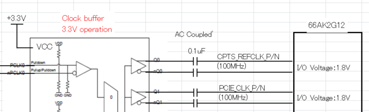


Is this acceptable?

Thanks and regards,
Koichiro Tashiro

  • Hi Koichiro,

    The output of the clock buffer must meet the voltage requirements specified in Table 5-5 which specifies the the voltage level must not exceed 1.8V. You will need to check the specification for the clock buffer to see if that requirement is met.  In addition AC coupling is not needed when connecting an LVDS compatible buffer, however, if the buffer specifies a termination circuit that circuit needs to be added.

    Regards, Bill

  • Hi Bill,

    Customer understood the voltage level mismatch between the clock buffer and K2G.
    The AC coupling is used to remove DC component, then only AC component (voltage swing) is passed on.

    Below TI application note described some examples to connect different voltage levels with AC coupling.
    https://www.ti.com/lit/an/scaa059c/scaa059c.pdf

    Is this approach not acceptable for K2G?

    Thanks and regards,
    Koichiro Tashiro

  • Hi Koichiro,

    I don't have any information on the buffer so I can't comment on whether it would be compatible. The only information you provided was that the buffer was operating at 3.3V.  If the LVDS signal is operating with a 3.3V swing it will violate the voltage limits for the signal regardless of AC coupling.  In addition the AC coupling assumes that the input buffer has the circuit to set the input reference voltage.  While this was true for clock buffers in previous parts, it is not listed as a feature for this one. 

    Regards, Bill

  • Hi Bill,

    I see. I will try to get the driver information from customer.

    >  While this was true for clock buffers in previous parts, it is not listed as a feature for this one. 

    Could you explain above sentence a bit more details?
    Do you mention about the LJCB in 66AK2Hxx devices?
    The document (Hardware Design Guide for Keystone II Device : SPRABV0) is not applicable for K2Gxx?

    Thanks and regards,
    Koichiro Tashiro

  • Hi Bill,

    Here are the driver information.

    IDT8SLVD1208-33I
    https://www.idt.com/us/en/document/dst/idt8slvd1208-33i-datasheet?language=en

    LVDS output DC characteristics are below.
    It seems the voltage swing is within 66AK2G12 specificaiton.


    Thanks and regards,
    Koichiro Tashiro

  • Hi Koichiro,

    The input clock buffer for the K2G component is an LVDS clock buffer.  This is different than the previous K2 components which used the LJCB clock buffer which required AC coupling.  The LVDS driver you have referenced is within the voltage limits of the K2G input clock buffer.  You will still have to include the clock termination circuit appropriate for the clock driver you have selected.  

    Regards, Bill

  • Hi Bill,

    Do you mean the AC coupling is not needed as the LVDS driver meets K2G input voltage limit?

    > You will still have to include the clock termination circuit appropriate for the clock driver you have selected.

    Do you mean the appropriate clock termination is the one described in page#14 in the datasheet?
    IDT8SLVD1208-33I
    https://www.idt.com/us/en/document/dst/idt8slvd1208-33i-datasheet?language=en


    Thanks and regards,
    Koichiro Tashiro

  • Hi Koichiro,

    AC coupling is not needed.  For your clock buffer the standard termination only requires a termination resistors between the positive and negative legs.  That termination is internal to the K2G so you should be able to connect the driver to the K2G input pins without any other termination.  You may want to include pads for an external resistor to allow additional to be added but it shouldn't be required.

    Regards, Bill